


レジスタ転送レベル(RTL)設計とは
レジスタ転送レベル(RTL)設計は、デジタル回路の設計プロセスにおいて不可欠なステップです。このステップでは、回路の物理的レイアウトを指定する前に、抽象レベルでデジタル設計の論理機能を定義して最適化します。エンジニアは、VHDLやVerilogなどのハードウェア記述言語(HDL)を使用して、設計全体での望ましい挙動をソフトウェアコードに変換します。
RTLレベルでモデリングできる最初のHDLは、1980年代に開発され、電子回路のデータフローをモデル化できるフル設計システムへと大きく変化を遂げました。
設計がより大規模かつ複雑になり、製造技術の発達によって論理演算や算術演算の新しい手法が開発されるにつれて、RTL設計手法も徐々に進化し、現在ではシステム仕様と回路設計ステップを橋渡しする、デジタル設計プロセスにおいて不可欠なステップとなっています。
RTL記述は抽象的であるため、より複雑で時間のかかる設計に取り掛かる前に、最適化された設計を得るための迅速な解析や設計反復を行えるようになります。
RTL設計は集積回路設計サイクルの重要な部分であり、エンジニアは物理的なコンポーネントやその接続方法を考える前に、レジスタ、演算、およびデータフローの各段階で設計を最適化できるようになります。この記事では、まずRTL設計の基礎について説明し、デジタル回路の設計への適用方法やRTL設計フローについても解説します。その後で、RTL設計がフィールドプログラマブルゲートアレイ(FPGA: Field-Programmable Gate Array)や特定用途向け集積回路(ASIC)にどのように適用されるか、そしてRTL設計の可能性についても説明します。
RTL設計の基礎
「レジスタ転送」とは、言語でレジスタ間のデータフローを記述して、論理演算や算術演算をデータに適用する方法を指します。エンジニアは、RTL設計を使用して機能ブロックを記述し、特定の機能を実行するために使用される個別のコンポーネントの挙動を定義します。各機能ブロックには、「順序回路」と呼ばれるブロック内のレジスタと、機能ブロックの論理演算を含む組み合わせ回路の記述が含まれています。また、HDLを使用して、回路を通過するデータの流れを定義するために、機能ブロックがどのように接続されるかを記述します。
RTL設計の利点は、複雑なシステムを、HDLコードで表現した比較的単純なブロックに分割できることです。ここでは、RTL設計の使用方法を理解する上で重要な基本事項をいくつか紹介します。
レジスタ
RTL設計では、一定量のデータを格納できるハードウェア要素を「レジスタ」と呼びます。通常、これらはDフリップフロップとして実装されます。レジスタの値は、論理演算への入力として読み込むことも、演算の出力として設定することもできます。レジスタ間でデータがどのように流れ、演算によってデータがどのように変化するかを特性付けすることが、RTL設計の基本的な目的です。
ハードウェア記述言語(HDL)
RTL設計で最も重要な部分は、回路の挙動を記述するコードです。HDLはプログラミング言語によく似た仕様言語で、変数、関数の呼び出し、if-then-elseやCASEのような論理文、ブール式、数学を使用します。ただし、HDLは電子回路(一般的には集積回路)の挙動と構造を記述するために特別に設計されています。HDLとプログラミング言語の違いは、時間の概念が言語内に含まれていることで、回路内のクロックで動作をトリガーできる点です。
これは、回路内のデジタルクロックの値を定義する変数を使用することで実行できます。この単純なインバータを記述したVHDL例では、クロック値clkがロー状態からハイ状態(立ち上がりエッジ)になると、出力(Q)が入力値(D)に設定されます。
D <= not Q;
process(clk)
 begin
     if rising_edge(clk) then
         Q <= D;
     end if;
 end process;
最も一般的に使用されているHDLであるVery High-Speed Integrated Circuit Hardware Description Language(VHDL)は、C言語とは異なる構文を持つ、強く型付けされた言語です。VHDLは、より複雑なシステム設計を記述するために推奨されるHDLです。
もう1つの一般的なHDLは、Verilogまたはその上位集合であるSystemVerilogです。より簡潔で、弱く型付けされ、柔軟性があり、構文はCコードに似ています。簡単に習得でき、すぐに記述できるため、多くのエンジニアが作業の開始時やそれほど複雑でない回路を扱う場合に利用しています。IEEEでは、VerilogとVHDLの両方を業界標準として定義しています。
ここでは、各言語でのANDゲートの単純な例を示します。ANDゲートには、2つの入力と1つの出力があります。入力が両方とも1の場合、出力は1になります。これらが等しくない場合、または両方が0に設定されている場合、出力は0になります。
VHDLでは、ANDゲートを次のように記述します。
entity my_and is -- First, you define the entity
   port (
      inp1: in  std_logic; -- The first port
      inp2: in  std_logic; -- The second port
      rst: out std_logic   -- The output port
   );
 end my_and;
architecture blk of my_and is -- Next, define the architecture
 begin
   process(inp1, inp2) -- With the inputs, do the following
   Begin
     -- Use a simple if-then-else statement
     if((inp1=’1’) and inp1=’1’))then
       rst <= ’1’;
     else
       rst <= ’0’;
     End if;
   end process
 end blk;
Verilogでは、ANDゲートを次のように記述します。
module my_and(inp1,inp2,rst); // define the module call
 input inp1, inp2;             // define inputs and output
 output rst;
assign rst = inp1 & inp2; // use the & (and) operator
endmodule
この論理演算では、2つの入力ポートにおける値を受け取り、両方のポートが1の場合、出力を1に設定します。これは単純な例ですが、このタイプのコードでシステム内のすべてのエンティティを表すことができ、それらを組み合わせてデジタル回路全体を定義することができます。代表的な基本構成ブロックとしては、加算器、乗算器、カウンター、メモリ、およびステートマシンがあります。設計エンジニアは、システムを定義すると、コードをコンパイラに送ります。エラーなしでコンパイルされた場合、エンジニアはその結果を使用してシステムをテストできます。
論理演算
RTL設計には、2つのタイプの演算があります。1つ目の論理演算では、レジスタに格納されたデータのビット評価と修正を行います。AND、OR、NOT、XOR、およびシフトなどの論理演算は、HDLで論理的な挙動を定義することで作成されます。上の例は、VHDLとVerilogでANDをどのように表現できるかを示しています。論理演算は、ハードウェア内の論理ゲートを表します。
算術演算
RTL設計における2つ目の演算タイプは、算術演算です。レジスタ内のデータを取得して、加算、減算、乗算、除算を行います。これらは、HDLでは標準的な算術演算子を使用して表現されます。例として、VHDLで2つの数値を加算する場合は、次のように記述します。
rst <= inp1 + inp2;
ここで、inp1とinp2は2つの入力レジスタであり、rstは出力レジスタに割り当てられます。RTLの算術演算は、加算器、減算器、乗算器、除算器などの専用の物理要素を表します。
同期および非同期アクション
RTL設計は、同期または非同期のいずれかの方法でデータの流れを表現できます。同期の場合、ルーチンは関数へのシステムクロック入力によって実行またはトリガーされます。非同期の場合、1つまたは複数の入力ポート値が特定の方法で変化したときにルーチンが実行されます。これは、クロック入力または非クロック入力の入力値を確認して、if文で変更されたかどうかを確認することで実装されます。
集積回路設計におけるRTLの役割
最新の集積回路(IC)設計フローでは、デバイスで実行すべき機能の仕様をパッケージ化された半導体チップに変換する必要があります。RTL設計がもたらす抽象化レベルにより、エンジニアは設計を物理的に実装する方法の詳細を考慮することなく、システムの上位レベルの機能に集中できます。
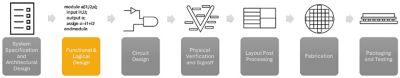
集積回路の設計プロセス。RTL設計は、システム仕様と回路設計ステップを橋渡しする。
IC設計フローの最初のステップは、システム仕様とアーキテクチャ設計を定義することです。この情報はHDLコードに変換されます。エンジニアは、そのコードを使用して機能設計と論理設計を定義します。定義が完了すると、設計はネットリストに変換され、それを使用して回路設計が作成され、その後に残りの設計プロセスが続きます。
RTL設計を使用した抽象表現は、物理設計、物理設計の検証、または実際の製造に時間とコストを費やす前に、設計プロセスのできる限り早い段階で行われます。RTL設計ステップをプロセスに組み込むには、開始時のシステム仕様と、RTL設計が完了したときにレジスタ、演算、およびデータフローを実際の回路に変換するツールとの間で、適切に統合する必要があります。
RTL設計フロー
RTL設計フローの目標は、集積回路(通常はFPGAまたはASICデバイス)の機能を定義して最適化することです。設計エンジニアは、RTL設計フローを使用して、まずデバイスのロジックとフローを定義し、システムをテストおよび最適化して、RTL定義をネットリストに変換します。一般的なRTL設計手法は、以下の5つのステップで構成されます。
1. 高レベルの合成
フローの最初のタスクは、最小限の編集でデバイスの仕様をHDLコードに変換することです。多くのケースで、エンジニアはCやC++などの標準プログラミング言語を使用してデバイスの望ましい挙動を表現します。次に、ソフトウェアツールを使用して、ソフトウェアモデル内のアルゴリズムを、選択した仕様言語に分解します。単純な設計ではこのステップを省略できますが、複雑な設計の場合はこのステップを踏むことで労力を大幅に削減できます。
2.RTLコーディング
このステップでは、エンジニアがコードを作成または改良します。設計者は、特定のレジスタ、必要な演算、データフローの詳細を記述します。このステップの重要な部分の1つは、モジュールを使用して、システムの一般的な演算や特定の部分を記述することです。モジュールが作成されると、必要に応じて再利用できるため、設計全体の複雑さが大幅に軽減されます。
3.性能、電力、面積(PPA)の最適化
コーディングが完了すると、最適化プロセスが開始します。このステップの目標は、性能を向上させ、消費電力を最小限に抑え、製品の物理的なサイズを抑えることです。
タイミングおよびロジックシミュレーション
シミュレーションツールを使用して、システム全体でタイミング解析を実行し、レジスタ値を追跡します。レジスタ転送レベルで設計のチェックを実行し、回路全体でタイミングの問題がなく、期待される出力が演算で生成されるかどうかを確認します。設計チームは、設計プロセスのできる限り早い段階で、システム内の電力グリッチなどの問題をデバッグします。
消費電力の予測
システム内のどのデバイスも、ある程度の電力を消費します。設計エンジニアは、消費電力量を把握し、設計を反復して、電力の供給状況を理解し、消費電力を最小限に抑える必要があります。Ansys PowerArtist™は、レジスタ転送レベルでの解析、プロファイル化、電力削減を行うために、多くの大手半導体設計企業で採用されています。Ansys PowerArtistを使用することで、設計チームは電力を詳細に解析し、電力効率の低いRTLコードを特定して、設計内の無駄なトグルをすべて特定できるようになります。
面積の最小化
どんなに小さなコンポーネントでも、その大きさに応じたスペースを必要とします。また、コンポーネント間の配線も同様です。RTL設計プロセスでは、コンポーネントの物理的なサイズは考慮されず、コンポーネント数とコンポーネント間の接続の複雑さが捕捉されます。
4.検証
設計の最適化が完了すると、すべての仕様が満たされていることを確認する必要があります。これは設計プロセスの重要な部分であり、設計をさらに進める前にすべての設計要件を確認する必要があります。これは、RTLシミュレーションまたは形式検証のいずれかを使用して行われます。
RTLシミュレーション:設計を多様な視点から検証するために、さまざまなソフトウェアツールを使用します。入力ベクトルを与え、結果の出力ベクトルを想定された結果と比較します。入力と出力は、通常は波形として表現されることで、設計エンジニアはシステムの挙動を視覚的に確認できます。
形式検証: これは自動化を使用して、一連の挙動予測を、システムの動作空間全体を探索する数学アルゴリズムに変換する静的な検証プロセスです。結果の正確さを確認するために、数学的に評価します。
5.RTL合成
システム設計の完全な検証が完了すると、RTL合成を使用して、RTL設計のHDLコード表現をゲートレベルのネットリストに変換します。これは、結果の回路図を電子設計自動化(EDA)ツールの物理レイアウトに変換するツールのための前工程です。Synopsys社などの企業は、EDAプラットフォームに組み込まれるさまざまな合成ツールを開発しています。
FPGAおよびASIC設計フローでのRTL設計の使用
集積回路は2つのクラスに分けられます。1つ目は、特定用途向け集積回路(ASIC)で、特定の用途またはタスク向けにカスタム設計されています。一度製造されると、チップ内のロジックは変更できません。ASICチップの例としては、メモリモジュール、デジタルボイスレコーダー、最適化された信号プロセッサ、マイクロプロセッサ、中央処理装置(CPU)、さらにはI/O、CPU、メモリなどを含むシステムオンチップのような複雑なものがあります。
2つ目は、フィールドプログラマブルゲートアレイ(FPGA: Field-Programmable Gate Array)チップで、製造後に再プログラム可能な半導体チップです。チップ内のジオメトリにロジックが組み込まれる代わりに、FPGAにはプログラミング可能な接続グリッドで接続された多数の論理ブロックが含まれています。
RTL設計は、両方の設計フローの最初の部分で同じ役割を果たします。RTL合成が完了すると、ASIC設計フローでは、エンジニアが物理回路を計画してレイアウトする必要があります。これは「フロアプラン」と呼ばれます。FPGA設計では、RTLコードは、利用可能な論理ブロックを認識し、それらのブロックを適切に配置して、ステップを配線するネットリストに直接変換されます。
これからのRTL設計
1970年代から1980年代にかけて、デジタルシステムの望ましい挙動を表現するためにハードウェア記述言語が使われ始めました。超大規模集積(VLSI)の採用が増え、IC設計のさらなる発展にも対応し続けたことで、ハードウェア記述言語も広く普及しました。集積回路のサイズがますます縮小し、クロック速度が高まる中、1つのチップに組み込まれる機能はさらに増加傾向にあるため、設計エンジニアはより多くの課題に直面しています。
設計の複雑さは緩和されないため、RTLツールを導入してこれらの課題に対応する必要があります。設計者が次世代の集積回路を定義するために使用するツールスイートを開発する企業は、RTL設計フローの使いやすさ、性能、そして機能を改善するための重要な事項に取り組んでいます。具体的には、以下の事項に注力しています。
- 電力低減
パワーマネジメントは、引き続き、集積回路の設計プロセス全体で最大の課題の1つとなります。システム内で電力を消費する電圧降下を理解して管理するためには、RTL最適化が必要となります。PowerArtistなどのツールが強化され、より多くのオプション、より優れた可視性、さらに高いスピードをもたらすことで、設計チームはこの課題に対処できるようになります。
- ツール間のシームレスな統合
設計、シミュレーション、検証、サインオフに使用できるツールの数が増えるにつれて、既存ツールの機能も増えます。これらのツールを提供する企業やIEEEのような業界団体は、規格を更新して改善し、ステップ間のフローを可能な限りシームレスにするツールを今後も提供していく必要があります。
- 設計フローへのAIの導入
集積回路設計プロセスで使用される多くのツールでは、機械学習(ML)やエキスパートシステムを使用して、特に物理回路のレイアウトでプロセスステップを高速化しています。改善されたMLアルゴリズムや、問題に対する最も可能性の高い次のステップや解決策を提案するための生成人工知能(AI)ツールの採用など、AIの導入は今後も増え続けるでしょう。
- 高レベル合成の改善
RTL分野のベンダーは、エンジニアが高レベルシステム仕様を、最適な構成に近い設計で、高レベルのハードウェア言語に高速に変換できるよう、懸命に取り組んでいます。
- よりスマートなRTL合成
RTLで記述されたゲートを、RTL合成ステップで実際のトランジスタに変換する際に、さらに生産性と最適化を大幅に向上できる余地はまだあります。物理的なジオメトリを設計に取り込む際に、情報に基づいた意思決定を行うことで、回路レイアウトの下流プロセスをさらに簡素化できます。