WHITE PAPER
Decoding Glitch Power at the RTL Stage:
A Shift-left Approach for Glitch Power Estimation and Optimization
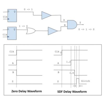
In the context of analyzing digital semiconductor circuits, a glitch is any unwanted or unused signal transition, or toggle. A glitch is often a transient signal that is much shorter than a clock period and therefore is not captured by the next register stage. We also encounter full transition glitches, or transport glitches, which refer to toggles in a data path circuit that cover a full clock period but do not contribute to the overall functionality of data path logic. These incidental toggles are considered unwanted and are termed “glitches.” The complexity of most chip designs means they generate a large number of glitches, which, like all transitions, briefly draw current and consume power. In this white paper, learn how Ansys PowerArtist™ software and the PowerArtist-SC™ platform can provide designers with a wealth of information on glitch power earlier in the design flow.