About this Webinar
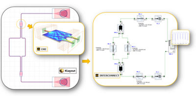
Photonic design workflows that connect layout tools with simulation tools are needed to verify designs before they are sent out for fabrication and are essential to achieving high yield. This webinar presents a photonic design ecosystem built on KLayout, Ansys Lumerical photonic simulation tools, and foundry process design kits (PDKs). To demonstrate these streamlined workflows, we'll design and simulate a custom multi-mode interference (MMI) splitter compatible with the AIM Photonics PDK process. Next, we'll extract the MMI compact model and develop a photonic circuit using a combination of the custom MMI and foundry-validated components. The webinar will walk you through all the steps for both the component and circuit-level design workflows.
What You Will Learn
- See the KLayout photonic layout features, including waveguide routing, port snapping, and DRC
- Understand the offerings of AIM Photonics PDK in Ansys/KLayout Platform
- Leverage the KLayout component design flow to simulate custom components easily
- Generate an accurate compact model for the custom-designed component to use in circuit simulation
- Launch circuit simulations directly from KLayout, using your custom component with other AIM Photonics PDK components
Who Should Attend
photonic circuit designers and engineers
Speakers
Guanhui Wang, Senior Application Engineer
Amit Dikshit, PDK Engineer/Design Enablement Manager, AIM Photonics


