-
United States -
United Kingdom -
India -
France -
Deutschland -
Italia -
日本 -
대한민국 -
中国 -
台灣
-
Ansysは、シミュレーションエンジニアリングソフトウェアを学生に無償で提供することで、未来を拓く学生たちの助けとなることを目指しています。
-
Ansysは、シミュレーションエンジニアリングソフトウェアを学生に無償で提供することで、未来を拓く学生たちの助けとなることを目指しています。
-
Ansysは、シミュレーションエンジニアリングソフトウェアを学生に無償で提供することで、未来を拓く学生たちの助けとなることを目指しています。
ANSYS BLOG
April 24, 2019
TSMC Certifies Ansys Multiphysics Simulations for Latest Advanced Packaging Technologies for SoIC
Ansys multiphysics simulations have been certified by the Taiwan Semiconductor Manufacturing Company (TSMC) to simulate its latest 3D integrated chip (3D IC) packaging technology for system on integrated chips (SoIC).
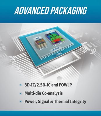
3D ICs are integrated circuits that consist of stacked silicon wafers, or dies, that are connected vertically using through-silicon vias (TSV) and/or through-dielectric vias (TDV).
There is also a popular variation of this advanced packaging technology — commonly referred to as 2.5D IC — which integrates heterogenous dies that are placed side by side on a silicon interposer within the same package.
Ansys multiphysics solutions are now certified for TSMC’s latest SoIC, CoWoS and InFO_MS advanced packaging technologies. It can simulate 3D IC, 2.5D IC, fan-out wafer-level packaging (FOWLP) and more.
These advanced packaging technologies improve the power efficiency and performance of high-speed cloud and data center electronics systems.
The TSMC certification of Ansys multiphysics simulations empowers customers to perform multi-die co-analysis and signoff for SoIC packaging technology. These simulations also enable:
- Power and signal net parasitic extraction.
- Power and signal integrity analysis.
- Power and signal electromigration analysis.
- Chip modeling for system-level power, signal and thermal integrity analysis.
- Thermal analysis estimations of the overall junction temperature variation of the die.
- Thermal-aware electromigration analysis.
- Thermal-induced stress analysis
“We’re pleased with the result of our collaboration with Ansys in delivery of TSMC-SoIC technology reference flow, which empowers customers to address growing performance, reliability and power demands for cloud and data center applications,” said Suk Lee, TSMC senior director, Design Infrastructure Management Division. “The collaborative efforts combining Ansys’ comprehensive chip-package co-analysis solutions with TSMC SoIC advanced chip stacking technology address complex multiphysics challenges in 3D IC packaging technologies.”
In addition to SoIC certification, Ansys multiphysics solutions have also been certified by TSMC for other packaging technologies including chip-on-wafer-on-substrate (CoWoS) 1.5 and integrated fan-out (InFO) with memory on substrate (InFO_MS) 1.0.
The Importance of TSMC Certification for Electronics Simulations
TSMC is a market-leading foundry. Engineers who design cloud and data center electronics systems using their advanced fin field effect transistor (FinFET) and 3D IC technologies need tools that are guaranteed to enable silicon and system success.
The Ansys chip-package-system ecosystem for power, thermal and signal integrity signoff
John Lee, general manager at Ansys, says, “Our 3D IC solutions address complex multiphysics challenges to meet the stringent power, performance, thermal and reliability requirements. Ansys’ comprehensive chip aware system and system aware chip signoff solutions empower mutual customers to accelerate design convergence with greater confidence.”
The Ansys software that has been certified by TSMC for SoIC, CoWoS and InFO_MS include:
- Ansys RedHawk
- RedHawk-CTA
- Ansys CMA
- Ansys CSM
Learn more about Ansys's solutions for PCB design and simulation.


?)