-
United States -
United Kingdom -
India -
France -
Deutschland -
Italia -
日本 -
대한민국 -
中国 -
台灣
-
-
產品系列
查看所有產品Ansys致力於為當今的學生打下成功的基礎,通過向學生提供免費的模擬工程軟體。
-
ANSYS BLOG
October 20, 2016
TSMC’s InFO Packaging Technology is a Game Changer, empowered by Ansys
For engineers designing integrated circuits (IC) including system on chips (SoC), using integration and miniaturization to increase performance and bandwidth while reducing power and footprint has been an ongoing, continuous strategy. Now TSMC has developed an InFO packaging technology that is truly a game changer!
Why is InFO technology a game changer?
As mobile phones and other handheld devices continue to be a key driver of semiconductor innovation, chips often go into systems that demand a small footprint and minimum height. Since wiring dimensions of a chip are much smaller than that on a board, a chip cannot be mounted directly on a board.
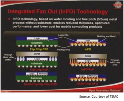
Instead, a substrate is typically used to spread and map the wiring between the chip and the board. With multiple chips, a larger substrate or even multiple substrates are needed, as in the current 2.5D, or 3D-IC packaging. On the other hand, TSMC’s InFO wafer-level packaging allows chip(s) (in the form of a die) to be mounted directly on a circuit board using wafer molding and metal. This eliminates the substrate and therefore reduces the height of the mounted chip.
In addition, multiple dies can be packaged together in one InFO package without the use of a traditional substrate between the dies and the PCB that the package is mounted on. This reduces not only the height, the footprint as well – allowing mobile devices to be thinner, lighter and more cost-effective.
According to TSMC, their InFO™ technology offers up to 20 percent reduction in package thickness, a 20 percent speed gain and 10 percent better power dissipation. Compared to current solutions, the much smaller footprint and cost structure of the InFO wafer-level packaging technology makes it an attractive option for mobile, consumer, automotive and IoT applications.
For any package technology, integrity, reliability and cost are three major vectors that need to be optimized. The integrity vector spans power and signal noise. Reliability deals with thermal, electromigration (EM), electrostatic discharge (ESD), electromagnetic interference (EMI) to thermal-induced structural stress issues. Cost factors in to almost all applications, and more so for consumer and the internet of things (IoT). Optimizing and ensuring the integrity and reliability of a chip (at a die-level) in the context of its respective package, board and system is very complex, even for the brightest engineers, especially when the chip uses advanced process nodes. The same analyses become even more complex when multiple dies are used as in a 2.5D or 3D-IC package such as InFO. The same is true when ensuring chip-aware system –level integrity and reliability.
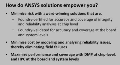
Ansys HFSS, known for its gold standard accuracy, works with Ansys Q3D, the 3D full-wave extraction capability to ensure integrity of high-frequency and high-speed designs at the board and system-levels. Thermal and structural issues are best solved using the thermal/stress simulation of Ansys Mechanical. In other words, Ansys solutions enable you to make sure your InFO-based design meets the integrity and reliability requirements at the chip, package and system levels.
At the chip level, Ansys RedHawk and Totem have been, and continue to be, the foundry-certified solutions for the last ten years, delivering the accuracy as stipulated by foundries, and minimizing field failures of silicon. RedHawk and Totem are both certified for TSMC’s latest 10nm and 7nm FinFET-based process technologies. RedHawk with its chip-package (CPA) and chip thermal (CTA) analyses, and DMP (Distributed Machine Processing) enable the creation of thermal and package-aware chips and hence products, ensuring the highest integrity and reliability.
Why is certification important, and what does it entail?
At the chip-level, the use of the latest process technology is typically driven by the need for one or more of the following: faster performance, greater bandwidth, higher performance to power ratio and reduced die size. The newer the process technology, the higher the opportunity for failure, and even greater is the cost of design mistakes. With the cost of creating a design using the latest process being tens of millions of dollars, risk of design failure is very high for the foundry, the design house and the tool supplier – Ansys. This is where the certification comes in.
TSMC and Ansys engineers worked very closely to ensure that all new rules, parameters and requirements for the 7nm process were considered by Ansys solutions and that the results correlated to their reference results from test silicon. Key capabilities within Ansys that enabled the certification include support for coloring, accurate modeling of multi-bit multi-height (MBMH) cells, modeling of special via structures, and associated complex electromigration (EM) rules. This level of certification criteria helps to ensure first pass silicon success.
TSMC first certified RedHawk in 2006. Since then RedHawk and Totem have maintained a consistent track record, earning the trust and certification for all TSMC process technologies with each and every release of technology design rule manuals (DRM). This illustrates the mutual confidence and trust between the two companies. The same confidence and trust have enabled Ansys to ensure that RedHawk and Totem are the signoff tools of choice for power integrity and reliability for the top semiconductor companies in the world. Thousands of successfully working production designs created over the last 10 + years are a testimony to RedHawk and Totem for their technical competence, and the trust placed by customers and foundry partners like TSMC.
Further validation through Partner of the Year Awards
In addition to the certification, TSMC validates Ansys and its solutions by bestowing two Partner of the Year awards at its Open Innovation Platform (OIP) event in San Jose, California in 2016. These awards are for:
- Joint Delivery of 7nm Mobile Design Platform and
- Joint Delivery of InFO Design Solution
Ansys continues to strive to earn that trust and certification from foundries, through focused engineering collaboration and sustaining technological edge, to enable the best first-pass silicon success for mutual customers.
To learn more about Ansys solutions for IC and SoC design, please visit the following sections of our Website:


