-
United States -
United Kingdom -
India -
France -
Deutschland -
Italia -
日本 -
대한민국 -
中国 -
台灣
-
-
產品系列
查看所有產品Ansys致力於為當今的學生打下成功的基礎,通過向學生提供免費的模擬工程軟體。
-
ANSYS BLOG
May 13, 2022
The Looming Uncertainty That Threatens Chip Timing and Performance Below 7nm
In the 4th century BC, a nobleman living on the island of Sicily named Damocles got the opportunity to sit on the king’s throne for a day. He was surrounded by luxury on all sides, but hanging over his head was a heavy sword, suspended by only a single horsehair that could break at any moment. The story of the Sword of Damocles is relevant today for advanced chip designers as they move from 7 nanometers (nm) to 5 nm and below. The potential disaster they feel looming over them is tied to dynamic voltage drop (DVD) and the inability of modern design flows to completely eliminate that threat.
This story is all about managing a reliable supply voltage. Each time a standard cell switches, it draws a transient pulse of current across the power supply network, which leads to a transient voltage drop (V=IR). The more cells that switch at the same time, the higher the current draw and corresponding voltage drop. The major problem with DVD is that it can impair the proper functioning of a cell if too large. But more insidious is the impact that DVD has on timing. Even “acceptable” DVD will slow down the switching speed of the cell, thus impacting the path timing through it. If multiple cells along a critical path experience DVD slowdown, the path may fail timing. Traditionally, designers calculate the size of dynamic voltage drop by simulating the circuit with real activity vectors, often supplemented with “vectorless” activity (i.e., automatically generated vectors) in an effort to increase coverage.
Coverage is the heart of the problem. A simple definition of coverage is the ratio of all cells that actually switched at some point during the simulation. So, if every cell switches somewhere in the activity simulation, it is sometimes called 100% coverage. But that is deeply misleading because it does not consider all the possible combinations of neighboring cells that could be switching at the same time.
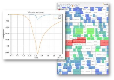
Self-induced IR drop is only a small fraction of the total dynamic voltage drop. Most of DVD is caused by simultaneous switching of cells placed near the victim cell.
Dynamic voltage drop is composed of two terms: there is the effect of the cell’s switching on its own supply voltage (self-drop) and the effects of nearby cells switching at the same time as a victim cell (neighbor-induced drop). With today’s technologies, self-drop is small, representing only about 15% of total voltage drop, and is completely dominated by neighbor-switching. The above simple definition of coverage is only 100% with regards to self-drop and does not capture the vast bulk of DVD caused by various combinations of neighbors switching.
A realistic coverage metric indicates what ratio of possible switching combinations have been exercised by the activity vectors. We can start to appreciate the challenge facing designers if we consider that the number of possible switching combinations is astronomical. Even if you consider only a small subset of cells, for example, when filtering down to just the 100 nearest cells surrounding a victim cell, that still leaves us with 2100 possible switching scenarios to consider for full DVD coverage.
Now, it is clear that not all of these combinations are realistic: The switching windows of the cells must overlap, and not all combinations are logically possible. Yet the activity vectors used today activate only a very small percentage of all realistically possible combinations, and real DVD coverage is estimated to be as low as 5-15%. That means that 85% of possible switching combinations remain unexplored.
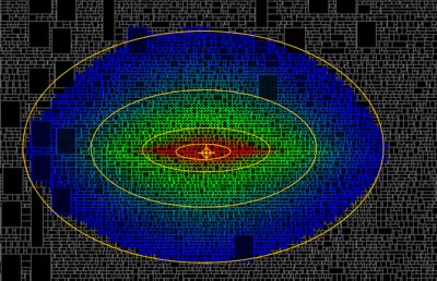
A zoomed-in view of cells placed near the victim cell at the center. The colors indicate the degree of electrical coupling through the power supply between a highlighted cell and the victim. Highly coupled cells will induce DVD on the victim cell if they happen to switch at the same time.
The reasons that DVD has become more sensitive to neighbor-switching emerged from three principal technology trends:
- Ultra-low supply voltages: Power consumption and system cooling have become some of the most important criteria when designing chips. The best way to reduce power consumption is to lower the supply voltage. This has led to the proliferation of ultra-low voltage processes operating down to just over half a volt. The result is that there is absolutely no room for deducting safety margins from the supply voltage. In earlier technologies, it was possible to eliminate voltage drop considerations by just assuming a worst-case IR drop across the board and assume every cell was running at less than nominal power – there was still plenty of supply voltage to adequately drive the cells. But those times are gone; every millivolt is precious if you want to hit the chip’s performance target.
- More coupled cells: Rising integration densities means that more cells are now electrically coupled in an area. This has led to a combinational explosion of possible switching scenarios that can generate significant power noise for any given victim. The switching of a large, power-hungry cell is now felt by more neighbors than before, worsening the coverage problem.
- Sensitive transistors: As transistors have shrunk, their performance has also become more sensitive to voltage level. The performance of library cells, especially the low-power versions, show a strong timing dependence on even small variations in supply voltage (VDD; i.e., dt/dV is bigger).
The simple solution would be to simply increase the number of simulated activity vectors so as to raise coverage. This is, unfortunately, infeasible. Simulating full-chip activity vectors is very computationally expensive. As few as 20 vectors can take half a day to simulate with multiple machines. Furthermore, it has traditionally not been possible to reduce the problem by simulating just the DVD impact on a few victim cells of interest. Activity vector simulation requires that the entire design be simulated for each vector.
This, in a nutshell, is the Sword of Damocles hanging over many designs today. Is there a switching combination out there — with just the right cells switching at just the right time — that will cause the chip timing to fail? Despite the luxuries at his fingertips, Damocles decided he preferred peace of mind and got off the king’s throne. But today’s chip designers have no good solution for DVD coverage and thus no choice but to keep sitting there and hope for the best.
As a technology leader in the area of power integrity research and solutions, Ansys has invested heavily in developing technologies to address DVD coverage and its impact on timing. Visit us at this year’s Design Automation Conference (DAC) to get a private peek at the latest thinking and beta releases from Ansys R&D on DVD and attend customer-led discussions on the state of the art in voltage drop analysis. Request a technical meeting or register to attend our DAC breakfast event.


