金屬氧化物半導體場效電晶體 (MOSFET) 的閘極電阻是極為重要的參數,尤其是在高頻、先進的半導體節點 (16 nm 及以下)。閘極電阻決定了 MOSFET 和互補金屬氧化物半導體 (CMOS) 電路的許多特性,例如:
- 切換速度
- RC (電阻電容) 延遲
- Fmax:振盪的最大頻率
- 閘極 (熱) 雜訊
- MOS 電容器和變容器 (壓控電容器) 中的串聯電阻和品質因數
- 功率場效電晶體 (FET) 的切換速度和一致性
但由於寄生電阻、電容、電感等複雜因素,確定這些節點的實際閘極電阻大小是困難的。寄生效應是指由於設計佈局和材料的物理缺陷,導致電路設計中存在多餘的電阻、電容或電感效應。顧名思義,寄生效應可能會導致功率損耗和過熱,也會降低訊號品質。為了更清楚理解閘極的運作,必須從模型中萃取這些寄生效應,以獲得電阻、電容和電感的實際數值。
專門的電子設計自動化 (EDA) 工具,例如 Ansys ParagonX 積體電路佈局寄生分析和除錯軟體,可透過視覺化佈局後網表的電阻電容 (RC) 網路連接來分析閘極電阻,例如 SPEF (標準寄生交換格式,是 IEEE 標準) 和 DSPF (詳細標準寄生格式)。這些工具可探測網表以查看並檢查 R 和 C 值,以及執行其他電力分析。SPICE 模型也相當實用,但由於寄生萃取方法「知道」佈局,因此被認為可以更準確地計算裝置周圍的寄生 R 和 C 值。
閘極電阻已有許多相關研究。然而,對於 IC 設計師和佈局工程師的實際工作而言,一些重要問題尚未受到討論或解釋:
- 寄生萃取工具如何處理閘極電阻?
- 如何從佈局或已萃取的佈局後網表評估閘極電阻?
- 如何識別閘極電阻是受到「固有」閘極電阻 (閘極多晶矽) 還是閘極金屬化繞線的限制,以及哪些是最關鍵的層和多邊形?
- 在製程設計套件 (PDK) 的 IC 設計流程中,是否捕捉閘極分散效應 (單接觸多晶矽和雙接觸多晶矽分別為 1/3 和 1/12 的係數)?
- 晶圓廠 PDK 是否包含垂直閘極電阻元件?
- 閘極應該加寬還是縮窄才能降低閘極電阻?
在本文中,我們將嘗試闡明這些未經充分討論的問題,並為 IC 設計和佈局工程師提供見解,以深入瞭解其設計中的閘極電阻。
閘極電阻的定義與測量
閘極電阻是從驅動點 (即閘極埠或閘極驅動器) 到 MOSFET 閘極實例引腳的「有效」電阻,如圖 1 所示。實例引腳是 SPICE 模型的端子與電阻網路之間的連接點。
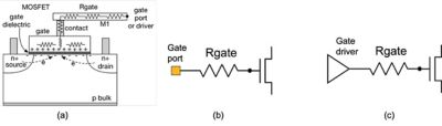
圖 1.MOSFET 横截面和閘極電阻示意圖
然而,圖 1 中簡單的示意圖可能會產生誤導。如圖 2 所示,閘極網路可以非常大,並包含許多驅動點、多個層 (金屬和通孔)、數百萬個多邊形以及高達數百萬個閘極實例引腳。
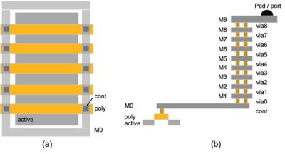
圖 2.MOSFET 閘極網路的俯視圖與橫截面示意圖
閘極網路是一個大型的分散式系統,具有一或多個驅動點和許多目標點。其外觀和表現都像一個巨大、規律的時脈網路,將閘極電壓分配給 FET。對於如此龐大且複雜的系統,導出等效且有效的閘極電阻並不是一件簡單明瞭的任務。SPICE 電路模擬不會明確報出閘極電阻值,因此需要使用寄生萃取工具。
寄生萃取工具處理閘極電阻
所有業界標準的寄生萃取工具都以類似的方式處理閘極電阻及萃取。在佈局中,MOS 閘極結構由傳統稱為「多晶」(多晶矽) 的 2D 遮罩表示,即使該材料可以由複雜的閘極金屬堆疊形成,並且可能具有複雜的 3D 結構。
寄生萃取工具基本上是在與主動 (擴散) 層的交點處截斷多晶矽線(圖 3 中的深灰色陰影區域) 。這會產生兩個可分析的部分:「閘極多晶矽」(主動區內的多晶矽,黃色陰影區域) 和「場多晶矽」(主動區外的多晶矽,淺灰色陰影區域)。多晶矽與主動區共同構成一個電晶體。
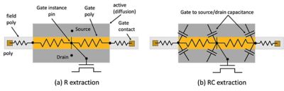
圖 3.MOSFET 閘極周圍的 R 和 RC 萃取
閘極多晶矽 (黃色陰影區域) 也在中心點處斷裂,並且 MOSFET (SPICE 模型) 的閘極實例引腳連接到閘極多晶矽的中心點 (黃色陰影區域中心的黑色垂直線)。閘極多晶矽由連接斷裂點的兩個寄生電阻表示。代表場多晶矽的寄生電阻連接到閘極接觸點或 MEOL (中段製程,由互連的金屬/通孔組成) 層,並進一步連接到上金屬層。
閘極多晶矽與源極/汲極擴散和接觸點之間的 MOSFET 外在寄生電容,由寄生萃取工具計算,並分配給電阻網路的節點。寄生電容連接到閘極電阻網路的細節可能會對瞬態和 AC 反應產生重大影響,尤其是在閘極寄生電阻非常大的先進節點。
這些細節會顯示在 DSPF 檔案中,但通常不會在公開文獻或晶圓廠 PDK 文件中討論。目視檢查文本 DSPF 檔案不僅繁瑣而且需要專業技術。ParagonX 應用程式等模擬軟體可用於視覺化佈局後網表的 RC 網路連接 (例如 DSPF、SPEF)、檢查 R 和 C 值、執行電力分析以及其他實用功能。
降階閘極模型
如圖 4 所示,MOSFET 閘極沿著閘極寬度形成一個大型的分散式 RC 網路。

圖 4.閘極沿閘極寬度的分散特性和模型
此分散式網路的 AC 和瞬態反應不同於簡單的集總單一 R 和單一 C 電路。研究人員顯示這類 RC 網路的運作方式與使用單一 R 與單一 C 元素1 的網路大致相同,其中:
- C 為總電容
- R=1/3 * W/L * rsh 適用於單面連接的多晶矽
- R=1/12 * W/L * rsh 適用於雙面連接的多晶矽
在這裡,W 是寬度、L 是長度,rsh 則是多晶矽的片電阻。係數 (1/3 和 1/12) 有效地實現準確的閘極降階模型,將大量 R 和 C 元素減少到兩個 (或三個) 電阻器和一個電容器。使用降階模型可簡化並加速寄生萃取軟體所執行的計算。
互連寄生對閘極電阻的影響
在較舊的節點技術中,金屬互連 (例如金屬和通孔) 的電阻非常低,閘極電阻則由閘極多晶矽主導。閘極電阻的分析和計算非常簡單。
當技術達到 16 nm 及以下時,互連具有非常高的電阻,並且可以大量 (50% 或以上) 貢獻至閘極電阻。根據佈局,閘極電阻可能取得來自任何層的大量貢獻,包括裝置 (例如閘極多晶矽或場多晶矽)、MEOL 或後段製程 (BEOL,由具有厚金屬和鈍化層的頂層組成)。
圖 5 顯示使用 ParagonX 軟體進行的閘極電阻模擬結果。柏拉圖 (圖 5a) 依照各層顯示電阻貢獻,有助於找出最重要的閘極電阻層。透過佈局多邊形可視化對閘極電阻的貢獻 (圖 5b),可立即指出閘極電阻的阻塞點或瓶頸,對於引導佈局最佳化工作非常有用。
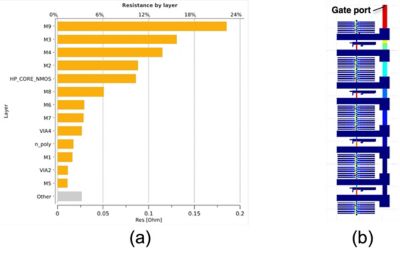
圖 5.閘極電阻模擬結果:(a) 各層的閘極電阻貢獻,以及 (b) 以顏色顯示佈局上多邊形的貢獻
FinFET 的閘極電阻
在平面式 MOSFET 中,閘極具有非常簡單的平面結構,閘極中的電流是沿著閘極寬度方向的一維流動。
在鰭式場效電晶體 (FinFET) 技術中,閘極環繞著非常高的矽鰭,形成複雜的 3D 結構。此外,根據功函數選擇閘極材料,即從固體表面移去一個電子到固體表面外側真空中的某一點所需的最小熱力學功,以調整臨界電壓。FinFET 的臨界電壓不是透過通道摻雜來調整,而是透過閘極材料來調整。這些材料具有非常高的電阻,遠高於所要求的多晶矽 (其典型片電阻小於 10 歐姆/平方)。此外,閘極可能由多層組成,例如具有矽的界面層和其上的一或多層。
但是,使用寄生萃取軟體時,IC 設計師和佈局工程師看不到這些細節。他們會看到「多晶矽」和「主動區」的一般多邊形,讓設計工作變得更輕鬆。
閘極電阻的垂直元件
在 16 nm 之前的技術中,閘極電阻由橫向電阻主導。然而在先進技術中,閘極材料層之間有多個界面,導致龐大的垂直閘極電阻。此電阻與閘極多晶矽區成反比。它可以建模為額外的電阻器,將閘極實例引腳連接到閘極多晶矽的中心點,如圖 6a 所示。因此,當閘極變窄 (例如鰭的數量較少) 時,閘極電阻會下降,但在閘極寬度非常小時,閘極電阻會上升,如圖 6b2 所示。它展現特有的非單調行為。先前的經驗法則是「較窄的閘極具有較低的閘極電阻」,但現在不再適用。設計師和佈局工程師必須選擇最佳 (非最小) 的閘極寬度 (鰭的數量),以將閘極電阻降至最低。
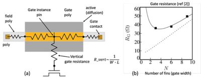
圖 6.(a) 考慮垂直閘極電阻的閘極模型,以及 (b) 經測量和模擬的閘極電阻與鰭數 (引自 [2])
科技趨勢
如我們所見,隨著技術讓節點越來越小 (目前低至 2 nm),閘極電阻和互連電阻都顯著增加,幅度達一個或兩個數量級。因此,在較舊的節點中對閘極電阻並不重要的佈局細節,在先進節點中變得非常重要。隨著節點尺寸持續縮小,此趨勢將繼續發展。為了瞭解這些層級的等效有效閘極電阻值,需要使用寄生萃取軟體,例如 ParagonX 軟體,因為 SPICE 模型在這些層級上不再有效。
進一步瞭解 ParagonX 軟體以改善您的 IC 設計流程。
參考資料
1.B. Razavi, et al., "Impact of distributed gate resistance on the performance of MOS devices," (分散閘極電阻對 MOS 裝置效能的影響) IEEE Transactions on Circuits and Systems I: Fundamental Theory and Applications, vol. 41, pp. 750-754, 11 1994。
2.A.J.Sholten et al., "FinFET compact modelling for analogue and RF applications," (類比和 RF 應用的 FinFET 經檢模型) IEDM 2010, p. 190。