Physics-based Analog Design Optimization
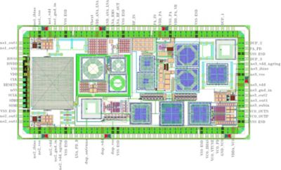
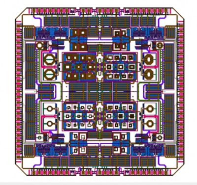
Learn about the revolutionary AI-driven electromagnetic-aware methodology of Ansys that automates the optimization of the floor plan of analog and RF physical layouts.
產品系列
查看所有產品Ansys致力於為當今的學生打下成功的基礎,通過向學生提供免費的模擬工程軟體。
Learn about the revolutionary AI-driven electromagnetic-aware methodology of Ansys that automates the optimization of the floor plan of analog and RF physical layouts.
Venue:
Virtual
Analog/RF IC design has been traditionally considered an art – sometimes even a “black art” – because, contrary to digital IC design, analog/RF design combines complexity, non-linearity, conflicting design objectives and limited automation in EDA tooling. Analog/RF IC designers rely on a blend of technical expertise, intuition, accumulated experience, and creativity to meet the demanding targets of modern applications like high operating frequencies, low power, miniaturization, and shrinking design cycles.
In this webinar you will learn about the revolutionary AI-driven electromagnetic-aware methodology that automates the optimization of the floor plan of analog and RF physical layouts. Join us to discover how Ansys AI solutions can add structure to the “madness” of analog/RF design.


Kelly Damalou, Product Manager, On-chip Electromagnetic Simulation