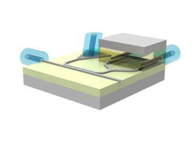
As optical systems become increasingly integrated, chip-to-chip and chip-to-fiber optical coupling have emerged as critical design challenges for photonic integrated circuits and co-packaged optics.
Join senior application engineers Yi-Hao Chen and Angel Morales, and guest MIT speaker, Drew Michael Weninger in our upcoming webinar for an in-depth presentation on optical coupling simulation methodologies, packaging design challenges, and the advantages and disadvantages of different techniques such as evanescent couplers, gratings, free form or edge couplers.
This webinar will introduce multi-scale simulation workflows using Lumerical FDTD, MODE, and Zemax OpticSudio to design a chip-to-fiber coupler with a large alignment tolerance. Learn how to use suitable solvers for establishing design constraints and optimizing taper geometry, alignment tolerances, wavelength and polarization response, and fabrication tolerances for high-volume manufacturing of chip-to-chip optical couplers.
What You Will Learn
- Develop a strategy for efficient and accurate modeling of optical coupler designs
- Learn multi-scale simulation workflow with Lumerical and Zemax
- Design and optimize a chip-to-fiber coupler with large alignment tolerance
- Design and optimize a novel chip-to-chip coupler design with overlapping inverse double tapers
Who Should Attend
photonic and optic designers and engineers
- Drew Michael Weninger, MIT, Electronic Materials Group
- Yi-Hao Chen, Senior Application Engineer
- Angel Morales, Senior Application Engineer


