-
United States -
United Kingdom -
India -
France -
Deutschland -
Italia -
日本 -
대한민국 -
中国 -
台灣
-
-
產品系列
查看所有產品Ansys致力於為當今的學生打下成功的基礎,通過向學生提供免費的模擬工程軟體。
-
ANSYS BLOG
September 30, 2020
Fraunhofer HHI Delivers its First SOA Compact Model with Ansys
The demand for discrete lasers, semiconductor optical amplifiers (SOAs) and photonic integrated circuits (PICs) is fueled by growth in leading-edge photonics technologies. Highly integrated photonic systems are necessary to meet demanding power and performance targets, with applications including biosensing, lidar for advanced driver-assistance systems (ADAS), connectivity for telecom and datacom networking, and emerging technologies in quantum and neuromorphic computing.
An MQW loaded ridge waveguide
forms the core of the Semiconductor
Optical Amplifier (SOA, left). On the
InP process, HHI can deliver a wide
range of active components, including
a PIN SOA with C-band PL peak shown
in the optical microscopy image of the
device (right).
Developing Compact Semiconductor Optical Amplifiers
Indium phosphide (InP) processes have long been a mainstay of integrated photonics, providing maximum functionality for PIC designers thanks to their support for native gain materials and lasers. As a leading InP foundry, Fraunhofer HHI is positioned to provide users with foundry services to achieve their most challenging design goals through experience and commitment to an open-access model.
The development of compact and efficient SOAs is a current focal point for the photonics industry. There is a need for system-level models calibrated to foundry measurements that enable engineers to leverage custom SOAs at the circuit level with the confidence their manufactured circuit will work as expected. The availability of compact models for SOAs has been limited by the complexity of the physics involved and the challenge of solving the problem efficiently. With a compact model that has been parameterized to HHI’s foundry now available, designers can avoid the costly effort of parameter extraction and calibration. The foundry-calibrated model gives designers flexibility while saving them the time and cost of iterations usually associated with customized advanced devices.
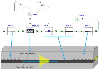
A variety of laser topologies can be modeled and simulated with the
traveling wave laser model (TWLM) in Ansys Lumerical INTERCONNECT
including FP, DBR, DFB, SOA/RSOA, Ring (Vernier) and Sampled gratings (Vernier).
Foundry Calibrated SOA Compact Models
HHI recently adopted Ansys Lumerical’s laser simulation solution, including the multi-quantum well (MQW) gain solver and traveling wave laser model (TWLM). The TWLM is an advanced time-domain compact model capable of capturing the full range of physics relevant to SOAs and lasers while achieving the simulation performance required for efficient analysis of complex PICs.
The development of the foundry-calibrated SOA compact model is the result of a close collaboration between HHI and Ansys Lumerical. With HHI’s state-of-the-art fabrication facilities, accurate and repeatable measurements of the devices were performed over wavelength, input optical power and input current. Based on these measurements — combined with simulation and fitting — parameters including active layer dimensions, recombination coefficients, modal gain, waveguide loss, and effective and group indices were extracted for the TWLM compact model. The results were compared to the measured power gain.
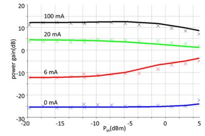
Using Ansys Lumerical INTERCONNECT as a simulation platform enabled the development and refinement of specific experiments to obtain key values for the compact model and accelerated the parameter extraction process through its support for automation. Simulation results using the compact model closely match the measured results from HHI.
Power gain vs. input optical power and current at C-band
center wavelength (1.55um). Simulated values shown as
solid lines, measured values shown as crosses.
Ansys is currently working with Fraunhofer HHI to simplify and accelerate the integration of light sources into integrated photonics design.
To learn more about HHI’s new compact model and Ansys Lumerical’s laser offering, register for the recorded webinar Ansys 2020 R2: Laser Simulation with Ansys Lumerical. The webinar will include an update on the 2020 R2 release.


