产品规格
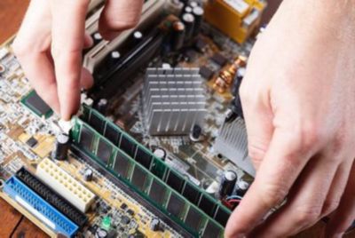
SIwave可帮助您对现代高性能电子产品中典型的高速信道和整个供电系统进行建模、仿真和验证。它可准确提取千兆位级的SERDES和内存总线,为各种产品的设计提供合规性签核。
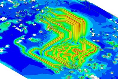
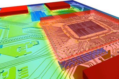
SIwave可帮助您对现代高性能电子产品中典型的高速信道和整个供电系统进行建模、仿真和验证。它可准确提取千兆位级的SERDES和内存总线,为各种产品的设计提供合规性签核。SIwave对完整配电网络(PDN)的全波参数提取使您能够验证噪声容限,并确保通过低电压设计中的自动去耦分析去满足阻抗特性。
SIwave可帮助您对现代高性能电子产品中典型的高速信道和整个供电系统进行建模、仿真和验证。它可准确提取千兆位级的SERDES和内存总线,为各种产品的设计提供合规性签核。
2025年1月
Ansys SIwave 2025 R1版本进行了功能扩展,增强了PI Advisor,优化了噪声和串扰分析,并加速了ECAD-MCAD工作流程的求解器性能,为PCB工程师和设计人员提供更高的速度和准确性。
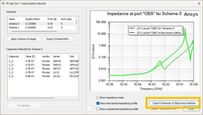
PI Advisor增强功能,可通过电源完整性仿真实现原理图生成自动化,从而简化了PCB电源完整性工程师和设计分析师的工作流程。该功能可简化分析,提高高科技、汽车以及航空航天产业的效率。
改进的求解器输入文件生成优化算法,从而可将大型项目的仿真时间缩短达5倍。该性能提升可在高科技应用中为PCB设计人员和仿真工程师的高效工作流程提供支持。
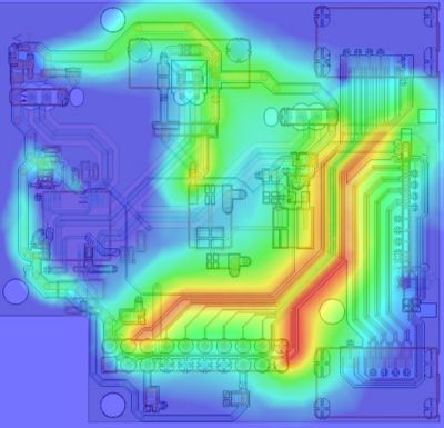
增强的噪声和串扰分析可为高速设计提供精确的深度洞察,从而帮助电路和PCB设计人员优化信号完整性。该功能可为Ansys SIwave的高科技和HPC领域的高级工作流程提供支持。
SIwave功能
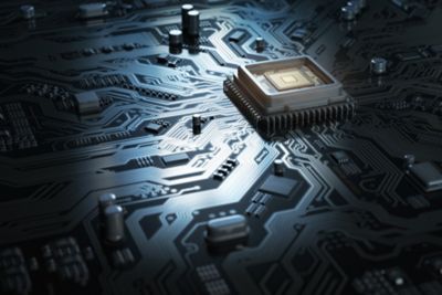
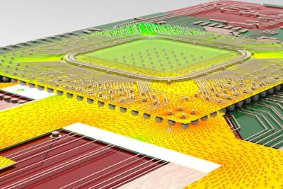
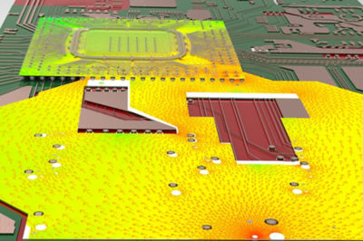
成功设计新一代电子产品需要电源完整性、信号完整性和热完整性协同分析。SIwave的独特功能可处理复杂地互连设计,从die-to-die,到IC、封装、连接器和电路板均可涵盖。
SIwave使电子公司能够以更快的上市时间、更低的成本和更高的系统性能获得竞争优势。
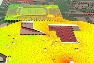
SIwave可帮助您在构建硬件原型之前就了解高速电子产品的性能。
SIWARE线缆资源与活动
了解如何通过利用SIwave中的HFSS区域来提高Ansys SIwave的速度和准确性,这是一项支持高速印刷电路板(PCB)信道设计要求的先进技术。
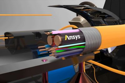
欢迎参加本次网络研讨会,届时将展示Ansys EMA3D Cable的新功能,以帮助您简化手动线缆设计。
要让包括残障人士在内的所有用户都能访问我们的产品,这一点对于Ansys而言至关重要。因此,我们始终致力于遵循基于美国访问委员会(第508节)、Web内容可访问性指南(WCAG)和当前自愿产品可访问性模板(VPAT)格式的可访问性要求。
如果您面临工程方面的挑战,我们的团队将随时为您提供帮助。我们拥有丰富的经验并秉持创新承诺,期待与您联系。让我们携手合作,将您的工程挑战转化为价值增长和成功的机遇。欢迎立即联系我们进行交流。