-
United States -
United Kingdom -
India -
France -
Deutschland -
Italia -
日本 -
대한민국 -
中国 -
台灣
-
-
产品组合
查看所有产品Ansys致力于通过向学生提供免费的仿真工程软件来助力他们获得成功。
-
ANSYS BLOG
January 8, 2020
Digital Image Correlation: A Key Technique for Materials Characterization
Digital image correlation (DIC) is a non-contact, full-field displacement, optical measurement technique. It is often used in the following applications:
- Materials characterization
- Coefficient of thermal expansion (CTE)
- Glass transition temperature
- Young’s modulus
- Poisson’s ratio
- Sample testing for fatigue and failure
- In situ monitoring of displacements and strains
- Displacement or deformation measurements
- High speed/frequency scenarios
- Crash testing, vibration
Diagram of a ball grid array (BGA). Engineers can use digital image correlation (DIC) to assess its thermal expansion or warpage due to thermal, mechanical
and thermo-mechanical loads.
DIC is an important tool to capture an electronic component’s response to simulated thermal, thermo-mechanical and mechanical loads. One of the best examples of the value of DIC is its ability to measure the CTE and warpage of ball grid array (BGA) devices.
How Thermo-Mechanical Loads Affect Ball Grid Arrays
A BGA is a complex semiconductor package consisting of multiple elements, including:
- One or more silicon dies
- A silica-filled epoxy encapsulant
- A layered composite of copper and glass fiber-reinforced epoxy
- Hundreds to thousands of solder balls
This complicated architecture, while necessary to meet performance and cost targets, can result in thermal expansion behaviors that can cause manufacturing defects and failure in the field.
Warpage results from a DIC
When the BGA is soldered to a printed circuit board (PCB) it can warp during reflow. This could result in solder defects, such as head-in-pillow (HiP), that can reduce first-pass yield and increase warranty issues.
While in operation, BGA power dissipation can heat up the package. If the BGA and PCB have different CTEs, the solder balls could experience stress that eventually results in fatigue, crack propagation and failures.
To help detect and prevent these issues, engineers use DIC because it is difficult to estimate warpage and CTE of these complex systems using other methods.
How to Perform a Digital Image Correlation of a Ball Grid Array
To better understand DIC, here is an example study engineers can use to learn how to measure the CTE and warpage of a dummy BGA.
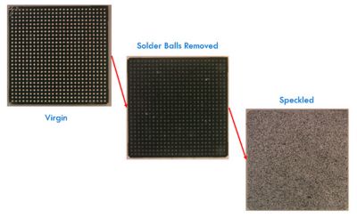
To learn how to perform a DIC, consider a BGA with a speckled pattern
and its solder balls removed.
First, the engineers prepare the sample for DIC by removing its solder balls with a soldering wick.
This is done because certain parts (like large lidded components and quad flat no-leads [QFN] overmolds) must be deconstructed and analyzed piece-by-piece.
Once the solder balls are removed, engineers speckle the part. This is done manually and requires a lot of practice. It’s important to make sure the base coat isn’t thick as this can throw off the readings. The speckles also need to be an appropriate size for the focal depth of the DIC cameras.
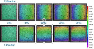
Engineers then put the speckled BGA into the camera chamber, which tracks how far apart the speckles move between different images, as the temperature changes. Engineers can use this information from the whole sample to estimate the CTE.
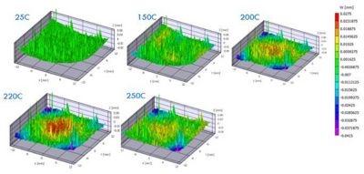
Plane displacement results from a DIC
How to Process the Data from a Digital Image Correlation of a BGA
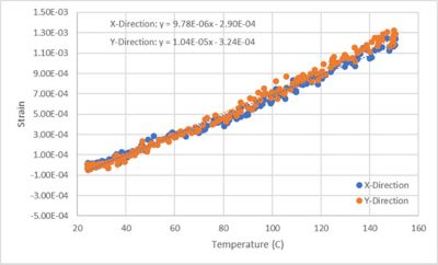
To assess the results from the DIC, engineers need to plot the BGA’s average strain against temperature.
A chart assessing the average strain versus temperature. The slope of 10 ppm/degrees Celsius (5.4 ppm/degrees Fahrenheit) is equal to the CTE.
If all goes well, a linear function can be fit to this data. In this case, the slope will represent the CTE.
In an in-house example, engineers found that the slope varied slightly over the temperature range. However, it can be stated with some accuracy, that the CTE is about 10 ppm/degrees Celsius (between temperatures of 20 and 150 degrees Celsius), or 5.4 ppm/degrees Fahrenheit (between 68 and 302 degrees Fahrenheit).
With this information, engineers can use Ansys simulation tools to assess if the particular BGA will fail during operation. To do this, they can plug the CTE and warpage profile into an Ansys Mechanical simulation to see if the warpage experienced at peak reflow temperature (250 degrees Celsius or 392 degrees Fahrenheit) will result in the solder ball separating from the solder paste.
In an in-house example, the total warpage, which is the absolute difference between the maximum negative and positive warpage, is 60 microns. This result can be evaluated by comparing it to the diagonal length of the BGA. If the percentage between the total warpage and diagonal length is below the industry standards of 0.3% or 0.7%, everything should be fine.
A more robust way to evaluate warpage is to place a model of the BGA on top of a model of the PCB and run a thermal-mechanical simulation within Mechanical. The total separation between the BGA and the PCB shouldn’t exceed 100 microns as this is larger than typical solder paste thickness.
A similar approach can be taken to mitigate risks at the customer level. The measured in-plane CTE can be input into Ansys Sherlock and then 1D and 3D simulations can be performed to predict the number of temperature cycles to failure.
DIC in combination with Ansys simulation tools provides engineers with deep insights into component manufacturability and reliability before final design and test. To learn more about DIC, register for the webinar: Ensuring Accurate Material Properties for Simulation with Digital Image Correlation (DIC).


