-
United States -
United Kingdom -
India -
France -
Deutschland -
Italia -
日本 -
대한민국 -
中国 -
台灣
-
-
产品组合
查看所有产品Ansys致力于通过向学生提供免费的仿真工程软件来助力他们获得成功。
-
ANSYS BLOG
May 26, 2016
Design of Advanced Driver Assistance Systems – A CPS Approach
An automobile is the biggest and most complex connected device used by consumers today. Advanced driver assistance systems (ADAS) is one of the fastest growing automotive applications. Stringent government requirements on automotive safety, fuel consumption and technology-focused consumer preferences are fueling the growth of ADAS. Driven primarily by safety, ADAS capabilities were first implemented in premium vehicles as key differentiators to enhance the user experience and protect the vehicle and its occupants. It started with features like parking assistance, adaptive breaking systems (ABS), adaptive cruise control and tire pressure monitoring.
Now, with capabilities like lane departure warning systems, driver alertness monitoring, blind-spot detection and obstacle detection, vehicles are better equipped to avoid collisions, protect pedestrians and enhance overall road safety.
The ADAS market has been estimated to be as high as $10 billion through 2018, with over 100 million units shipped by then. Since semiconductor components — the chips, packages, board and system, including firmware and software — are critical to building these advanced driver assist systems, research shows the related semiconductor market to be over $2 billion by 2018. A complete Chip-Package-System (CPS) flow is crucial to develop these advanced semiconductor devices. Ansys’ semiconductor and electronics system design solutions, with their silicon-proven track record, empower designers with a full chip-package-system solution for ensuring power noise integrity and — most importantly — reliability.
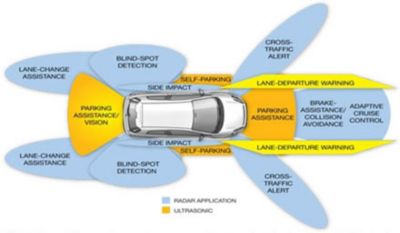
Several driver-assistance systems are currently using radar technology
to provide blind-spot detection, parking assistance, collision
avoidance, and other driver aids. Courtesy Analog Devices
The advanced system on chip (SoC) integrated circuits (ICs) at the heart of advanced driver assistance systems receive inputs from a variety of sensors in the vehicle itself (in-vehicle), as well as from other vehicles (vehicle-to-vehicle) and transportation infrastructure (vehicle-to-infrastructure). The sensor data comes from technologies such as ultrasonic, camera, (radio detection and ranging), LIDAR (light detection and ranging), GPS and IR (infrared). The need to detect, analyze and recognize every object — fixed and moving — around a vehicle in motion, under all lighting conditions, is paramount. This includes signs, people, animals, other vehicles, road barriers, and more.
To put it bluntly, in the history of semiconductors, no consumer application has had more of an effect on safety than the automotive ADAS application. A device failure will most probably lead to a destructive outcome. With that as the backdrop, every SoC with every IP (intellectual property) that goes into that SoC has to be designed for integrity and reliability. Apart from functionality and performance, this includes power integrity and reliability against thermal, electromigration (EM), electrostatic discharge (ESD) and electromagnetic interference (EMI) — all critical for automotive safety.
How does safety drive the design of such ADAS applications? This is best illustrated using an example. Consider a bicyclist riding along when all of a sudden the door of a parked car is opened directly in her path. To avoid crashing into the door, she veers slightly into the path of a car traveling just behind in the adjacent lane. The ADAS application in the traveling car has to, in real-time, recognize the cyclist, process and analyze data from all sensors (including ultrasonic, camera, RADAR, LIDAR, GPS and IR data) and either issue a warning to the driver, or better yet apply the brakes to avoid hitting the cyclist. This must be done in real-time, under any lighting conditions — a truly daunting challenge.
For a faster time to decision, the processing of data, including image recognition from multiple sources, must be done in hardware, not software. To ensure high-quality image recognition and fast time to decision, protocols like convolutional neural networking (CNN) algorithms are implemented into the SoCs based on advanced process technologies, thereby ensuring performance and bandwidth. While the advanced process technology offers higher performance and reduced power, the lower operating voltage associated with the process leads to lower noise margins, requiring tighter power noise integrity. Electrical noise is typically generated from fast switching digital circuitry, substrate noise from the coexistence of fast digital and highly sensitive analog circuitry on the same IC, the package and board. Too much noise could interfere with the performance and interpretation of data by an ADAS application. Thermal effects from on-chip current as well as the automotive environment can have a big impact on power integrity as well as reliability in terms of EM, ESD and EMI.
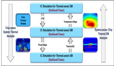
This is where Ansys simulation solutions come in. Ansys CPS simulations can ensure the tighter power noise integrity needed for ADAS applications. Ansys RedHawk, Ansys Totem and other electronic solvers in our product line can predict thermal effects, EM, ESD and EMI to help you design SOCs with less noise for image recognition in hardware. This graphic details all the ways that Ansys simulation can improve SOCs using CPS design flow:
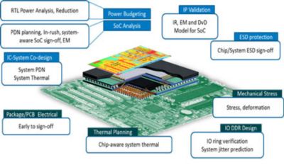
Any one of these factors could make the difference between the success or failure of your ADAS component or system. Why leave any one of them to chance? Explore our CPS capabilities in more detail here.


