-
United States -
United Kingdom -
India -
France -
Deutschland -
Italia -
日本 -
대한민국 -
中国 -
台灣
-
Ansys stellt Studierenden auf dem Weg zum Erfolg die Simulationssoftware kostenlos zur Verfügung.
-
Ansys stellt Studierenden auf dem Weg zum Erfolg die Simulationssoftware kostenlos zur Verfügung.
-
Ansys stellt Studierenden auf dem Weg zum Erfolg die Simulationssoftware kostenlos zur Verfügung.
-
Kontakt -
Karriere -
Studierende und Akademiker*innen -
Für die Vereinigten Staaten und Kanada
+1 844,462 6797
ANSYS BLOG
May 3, 2023
3D-IC Design: An Innovative Approach to Chip Integration
Advancements in technology have led to the development of increasingly complex and densely integrated circuits (ICs). To keep up with the ever-growing demand for high-performance and power-efficient devices, the industry has shifted toward 3D-IC design. 3D-ICs have many applications in a wide range of industries, including consumer electronics, telecommunications, computing, and automotive.
What Is 3D-IC Technology?
3D-IC technology refers to a range of packaging technologies for multi-die integrated circuits, in which multiple semiconductor chips — called “chiplets” — are placed close to each other (2.5D-IC) or stacked on top of each other (3D-IC). The chiplets are interconnected using a silicon interposer with through-silicon vias (TSVs), which penetrate through the silicon interposer and enable the connection between all layers. TSVs offer shorter interconnect lengths, lower parasitic capacitance, and higher bandwidth, leading to improved system performance. This technology allows heterogeneous integration of chips in areas such as logic, memory, sensors, microelectromechanical systesm (MEMs), and more in a compact form factor, leading to higher performance, lower power consumption, and reduced form factor.

Why Is 3D-IC Technology a Better Alternative?
System-on-chip (SOC) is the first choice for every IC designer as it offers higher performance and expanded functionality. But SOCs are monolithic, and integration of mixed elements into a single die delays product delivery and increases the overall cost of an IC.
There are several limitations to SOC design methods. One of the primary limitations is the size of the chip itself, since all the components of an electronic system are placed on a single chip. This means that the number and types of components that can be integrated onto a SOC are limited by the available space on the chip.
Another limitation of SOC design is the cost and complexity of the manufacturing process. As many components are integrated on a single chip, advanced semiconductor manufacturing processes are required, which can be expensive and complex. This can make it challenging to produce SOCs in large quantities and can limit their commercial viability.
Because all the components are tightly packed in an SOC package, this leads to increased power consumption and decreased performance. A high level of integration also limits the flexibility and upgradability of the system. Overall, while SOC design offers many benefits, such as smaller size and reduced complexity, it is important to carefully consider the potential limitations before deciding to use this approach.
The limitations noted above have encouraged designers to move toward a more revolutionary approach: 3D-IC design. This approach offers several advantages over traditional 2D-IC design, including increased performance, reduced power consumption, and a smaller form factor. 3D-IC design technology allows heterogeneous integration, more efficient use of space, and improved electrical performance compared to traditional 2D-ICs.
3D-ICs use silicon interposers and TSVs for better connectivity among different IPs. A silicon interposer is a thin wafer of silicon that is used in 2.5D and 3D-IC design to connect multiple dies or chips in a single package. It acts as a substrate on which dies are placed and connected using fine-pitch vertical TSVs and microbumps. This allows for better heat dissipation, reduced power consumption, higher density, and improved electrical performance compared to traditional 2D-ICs.
Design Challenges of 3D-ICs
There are several multiphysics challenges in 3D-IC design, including heat transfer, electromigration, stress and strain, and thermal expansion. These challenges arise due to the complex and interconnected nature of 3D-ICs, in which multiple dies are stacked on top of each other and connected using TSVs and microbumps.
Thermal expansion is also a challenge in 3D-IC design. As the temperature of an IC changes, different materials used in the IC will expand at different rates, causing stresses and warpage that can affect its performance and reliability. Heat transfer can further complicate the temperature distribution in the 3D-IC design. Due to the high density of transistors and other components, heat transfer gets difficult in 3D-ICs. Most of the heat is trapped in the system, which contributes to the increased temperature. This phenomenon is called self-heating. The 3D-IC constitutes billions of components that are connected through long interconnect wires. Joule heating resulting from these long connections is another major problem area that contributes to overall temperature increase. These heat sources must be monitored and analyzed when designing 3D-ICs to ensure reliable performance.

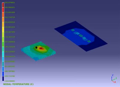
Thermal distribution in multi-die 3D-IC system
Ansys RedHawk-SC Electrothermal offers a gold-standard technology to examine and simulate the thermal behavior of a 3D-IC design using a silicon interposer. You can easily model the geometry and material properties of a 3D-IC design, including the silicon interposer, and simulate the heat transfer within the design. You can also easily analyze the temperature distribution and heat dissipation to see if the design meets required thermal performance specifications.
Electromigration is another major challenge in 3D-IC design. This refers to the movement of electrons within a conductor, which can cause damage to the IC over time. This is especially problematic in 3D-ICs due to the high currents and density of components, which can increase the risk of electromigration. Engineers can sign off electromigration reliability without thinking twice with Ansys Redhawk-SC.
Power integrity and signal integrity are always the top concerns of any IC designer. Power integrity signoff is more complicated in 3D-ICs due to their complex geometry. The relationship between power and temperature further complicates this. The power consumption of each block in the system is different, which creates different temperature distributions around each block. To optimize the power integrity of the system, the designer must overcome these multiphysics issues present in 3D-ICs. With Ansys software, it’s easy to generate power models for the blocks and simulate the behavior of the system.
3D-IC design is a revolutionary approach to chip integration that offers small form factor, but has many multiphysics challenges. Addressing these multiphysics challenges is crucial for successful design and implementation. Ansys tools have the capability to easily address challenges by offering best-in-class simulation technology. You can easily analyze signal integrity, power integrity, and thermal integrity of 3D-ICs to ensure that your design meets all required performance specifications.
Learn about RedHawk-SC and check out our related webinar "Thermal Integrity Challenges and Solutions of Silicon Interposer Design."


