


THEMENDETAILS
Was ist Plasmonik?
In den letzten Jahrzehnten wurden erhebliche Fortschritte in den Bereichen Elektronik und Photonik erzielt, die zu enormen Verbesserungen bei den Datenverarbeitungstechnologien geführt haben, die uns das Leben erheblich leichter machen.
Unter Plasmonik versteht man die Manipulation optischer Signale an Metall-Dielektrikum-Schnittstellen im Nanometerbereich (Milliardstel-Meter-Bereich). Inspiriert von der Photonik nutzt die Plasmonik die charakteristischen Eigenschaften metallischer Nanostrukturen, die die Weiterleitung von Lichtsignalen in nahezu atomarem Maßstab ermöglichen.
Die Integration herkömmlicher Photonik und Elektronik mit Plasmonik auf demselben Halbleiterchip bietet erhebliche Vorteile: superschnelle Computerchips und optische Kommunikationsgeräte sowie die Grundlage für ultraempfindliche Sensoren und Mikroskope.
Was sind Oberflächenplasmonen?
Als Professor Atwater vom California Institute of Technology 2007 den Begriff Plasmonik prägte, sagte er voraus, dass die Technologie eine Vielzahl von Anwendungen hervorbringen würde, von ultraempfindlicher Biosensortechnologie bis hin zur Realisierung von Unsichtbarkeit.
Unabhängig von der Anwendung beruht die Plasmonik auf der Manipulation von Wechselwirkungen zwischen elektromagnetischen Feldern und freien Elektronen an Metall-Dielektrikum-Schnittstellen. Ein Dielektrikum ist ein Isolator (wie Glas oder Luft), der durch die Anwendung eines elektrischen Feldes polarisiert werden kann. Freie Elektronen, die die elektrischen und optischen Eigenschaften von Metall bestimmen, oszillieren in Gegenwart elektromagnetischer Felder (z. B. Licht), was zu einem Phänomen führt, das als Oberflächenplasmonen bezeichnet wird.
Was ist Oberflächenplasmonenresonanz?
Im Nanometerbereich sind freie Elektronen auf winzige Bereiche des Raumes beschränkt, was den Frequenzbereich, in dem sie vibrieren können, begrenzt. Bei ihrer Interaktion mit dem Licht absorbieren sie das Licht, das ihren Schwingungsfrequenzen entspricht und reflektieren den Rest, was bedeutet, dass sie in Resonanz sind – daher der Begriff „Oberflächenplasmonenresonanz“ (auch bekannt unter der Abkürzung SPR für „surface plasmon resonance“). SPR kann in Nanostäbchen, Nanodrähten, nanophotonischen Elementen und anderen Arten der Nanotechnologie genutzt werden.
Die Technologietreiber der Plasmonik
Unsere datenorientierte Gesellschaft hat seit den ersten chipbasierten Halbleitern einen langen Weg zurückgelegt und produziert immer kleinere und schnellere Prozessoren. Zugleich bringt die ständig abnehmende Größe dieser Geräte eigene Herausforderungen mit sich, wobei thermische Problemstellungen und die Verarbeitungsgeschwindigkeiten der Entwicklung Grenzen setzen.
Optische Verbindungen bieten hier mit ihrer großen Bandbreite (Datenübertragungskapazität) eine vielversprechende Lösung. Die Beugungsgrenze des Lichts spielt jedoch eine wichtige Rolle, da sie der möglichen Verkleinerung photonischer Komponenten eine Grenze auf etwa die Hälfte der Lichtwellenlänge setzt. Daher sind photonische Geräte im Allgemeinen ein bis zwei Größenordnungen größer als ihre elektronischen Gegenstücke.
Es werden erhebliche Anstrengungen unternommen, um die einzigartigen Eigenschaften von Oberflächenplasmonen zu nutzen und die Größeneffizienz der Elektronik mit der Dateneffizienz der Photonik zu kombinieren.
Herausforderungen in der Plasmonik
Da ohmsche Verluste die Ausbreitung der Oberflächenplasmonen schon nach wenigen Millimetern dämpfen, werden zurzeit plasmonische Nanostrukturen aus plasmonischen Nanopartikeln wie Graphen, Metalloxiden und Nitriden untersucht.
Die Wärmeentwicklung stellt eine weitere Herausforderung dar. Sie kann die Ausbreitungslänge und Amplitude der plasmonischen Signale beeinflussen.
Mit Metallnanostrukturen und -geometrien, die die richtige Kombination von elektrischen und optischen Eigenschaften aufweisen, lassen sich diese Herausforderungen unter Umständen überwinden. Dies liegt daran, dass metallische Nanostrukturen in Kupfer, Silber, Aluminium, Gold und anderen Materialien die Ausbreitung von Oberflächenplasmonpolaritonen (SPPs, „surface plasmon polaritons“) ermöglichen.
SPPs sind resonante Elektronenschwingungen, die sich an Metall-Dielektrikum-Schnittstellen ausbreiten. Sie führen zu starken Licht-Materie-Wechselwirkungen, die bei optoelektronischen Anwendungen schwache optische Effekte verstärken können.
Plasmonische Wellenleiter
SPPs können als spezielle Arten von Lichtwellen angesehen werden. Daher verhalten sich metallische Verbindungen, die die Ausbreitung dieser Wellen an Dielektrikum-Metall-Schnittstellen unterstützen, wie optische Wellenleiter bzw. plasmonische Wellenleiter.
SPPs werden durch einen komplexen Wellenvektor dargestellt. Der imaginäre Teil dieses Vektors ist umgekehrt proportional zur SPP-Ausbreitungslänge, während der reelle Teil proportional zum Einschluss ist.
Die praktische Integration von Oberflächenplasmonen in die Schaltkreiskonstruktion hängt vom Ausgleich der inversen Beziehung zwischen Ausbreitungslänge und Einschluss ab. Im Idealfall maximieren plasmonische Wellenleiter sowohl den Einschluss als auch die Ausbreitungslänge von Oberflächenplasmonen, um eine optimale Wirkung zu erzielen.
Verlustleistungen, die natürlich aus der Ausbreitung von Oberflächenplasmonpolaritonen resultieren, können mittels Verstärkung oder durch die Integration photonischer Elemente wie Fasern kompensiert werden, was zu hybriden plasmonischen Wellenleitern führt.
Plasmonische Wellenleiter weisen Subwellenlängenmodalitäten auf, die unter der Beugungsgrenze des Lichts liegen. Der Gedanke, dass Ausbreitungsmodalitäten von SPPs mit Wellenlängen unterhalb der Wellenlänge von Licht möglich sind, hat für enormes Aufsehen gesorgt, da dies Geräte in Chipgröße möglich machen könnte, die eine Informationsverarbeitung mit optischen Frequenzen im Nanometerbereich ermöglichen.
Zu den gängigen Arten von plasmonischen Wellenleitern gehören Metall-Isolator-Metall-(MIM-), Isolator-Metall-Isolator-(IMI-), Kanal-Plasmon-Polariton-(CPP-) und Lücke-Plasmon-Polariton-(GPP-)Wellenleiter.
Was sind plasmonische Metamaterialien?
Ein Metamaterial ist ein Verbundwerkstoff, der so konzipiert ist, dass er Eigenschaften aufweist, die seine einzelnen Komponenten nicht haben. Metamaterialien leiten ihre Eigenschaften von ihren einzigartigen Größen, Formen, Geometrien und Ausrichtungen ab, die ihnen die Fähigkeit geben, elektromagnetische Wellen auf neue und vorteilhafte Weise zu beugen, zu blockieren, zu absorbieren oder zu verstärken. Metamaterialien sind in sich wiederholenden Mustern mit Wellenlängen, die kleiner sind als die der Phänomene, die sie beeinflussen wollen, angeordnet.
In plasmonischen Metamaterialien sind es die Oberflächenplasmonen, die diesen Materialien ihre einzigartigen Eigenschaften verleihen. Unter bestimmten Bedingungen koppelt sich einfallendes Licht mit Oberflächenplasmonen an Metall-Dielelektrikum-Schnittstellen und bilden sich selbst erhaltende, sich ausbreitende elektromagnetische Wellen, die als Oberflächenplasmonpolaritone (SPPs) bezeichnet werden.
Diese SPPs leiten ihre Eigenschaften aus der Struktur der zugrunde liegenden Metall-Nanopartikel ab. SPPs weisen bei Wellenlängen, die unterhalb der Wellenlänge des einfallenden Lichts liegen, fein austarierbare Eigenschaften auf. Beispiele für plasmonische Metamaterialien sind Gold-Nanopartikel (Nanowürfel) sowie Silber- und Gold-Nanoschalen in periodischen Anordnungen.
Arten plasmonischer Metamaterialien
Da plasmonische Metamaterialien ihre Eigenschaften aus der Anordnung von Metall-Nanopartikeln in Größenordnungen unterhalb der jeweiligen Wellenlänge ableiten, können Techniker*innen Eigenschaften wie Dispersion, Permittivität, Permeabilität und Brechungsindex manipulieren, um eine Reihe neuer Anwendungen zu ermöglichen.
Plasmonische Negativ-Index-Metamaterialien
Wenn Licht von einem Medium zum anderen, beispielsweise von der Luft ins Wasser, übergeht, wird es gebeugt, wenn es die Normale, also die Ebene, die im rechten Winkel zur Oberfläche liegt, durchquert. Bei Negativ-Index-Materialien erfolgt diese Beugung in die entgegengesetzte Richtung, was bedeutet, dass die elektromagnetische Energie des Lichts in eine Richtung transportiert wird, die der sich ausbreitenden Wellenfront entgegengesetzt ist.
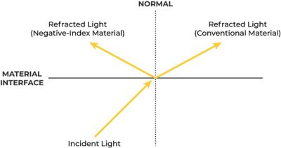
Da der Brechungsindex des Materials mit seiner Permittivität zu tun hat, die wiederum seine elektromagnetische Ausbreitungslänge beeinflusst, bieten Negativ-Index-Metamaterialien fein abstimmbare optische Eigenschaften, die über die Fähigkeiten herkömmlicher Linsen, Spiegel und optischer Geräte hinausgehen.
Plasmonische Gradienten-Index-Metamaterialien
Plasmonische Metamaterialien können auch so konfiguriert werden, dass sie über ihre Länge oder Oberfläche hinweg unterschiedliche Brechungsindizes aufweisen. Diese Art von Metamaterialien kann hergestellt werden, indem beispielsweise ein synthetisches Polymer wie PMMA mittels Elektronenstrahllithographie auf einer Gold-Nanooberfläche aufgebracht wird.
Plasmonische Gradienten-Index-Metamaterialien sind etwa zum Einsatz gekommen, um Lüneburg- und Eaton-Linsen herzustellen, die mit Oberflächenplasmonpolaritonen interagieren anstatt mit konventionellen Photonen aus Licht.
Es wurden auch schon dreidimensionale Negativ-Index-Metamaterialien vorgeschlagen, die möglicherweise durch Selbstmontage, mehrschichtige Dünnschichtabscheidung und fokussiertes Ionenstrahlfräsen hergestellt werden könnten.
Metamaterialien mit negativem Strahlungsdruck
Wenn Licht auf konventionelle Materialien leuchtet, d. h. solche mit positivem Brechungsindex, entsteht ein positiver Strahlungsdruck, d. h. das Material wird von der Lichtquelle weggeschoben. Der gegenteilige Effekt tritt bei einem Negativ-Index-Material auf, d. h. das Material wird von der Lichtquelle angezogen.
Dies könnte beispielsweise zur Erhöhung der Energieübertragungseffizienz und der Lichtabsorption beim Betrieb von Lichtquellen und Lasern oder zur Verbesserung der Lichtabsorption in Dünnschicht-Solarzellen genutzt werden.
Hyperbolische Metamaterialien
Hyperbolische Metamaterialien verhalten sich abhängig von der Bewegungsrichtung des Lichts als Metall oder als Dielektrikum. In diesem Fall bildet die Dispersionsrelation des Materials ein Hyperboloid, was (theoretisch) zu unendlich kleinen Ausbreitungswellenlängen führt.
Hyperbolische Metaoberflächen wurden schon auf Silber- und Gold-Nanostrukturen demonstriert. Diese Strukturen liefern verbesserte Funktionen (negative Brechung, Beugungsfreiheit und mehr) für Sensorik und Bildgebung. Daher haben diese Strukturen vielversprechende Anwendungen in der Quanteninformationsverarbeitung als Teil optischer integrierter Schaltkreise.
Darüber hinaus können hyperbolische Supergitter aus der Kombination von kompatiblen Kristallstrukturen wie Titannitrid und Aluminium-Scandium-Nitrid gebildet werden. Im Gegensatz zu Gold und Silber sind diese Materialien mit vorhandenen CMOS-Komponenten kompatibel und bei höheren Temperaturen thermisch stabil. Da sie eine höhere photonische Dichte aufweisen (im Vergleich zu Gold oder Silber), sind sie auch effiziente Lichtabsorber.
Hyperbolische Metamaterialien eröffnen Möglichkeiten wie planare Linsen mit erweiterten Sensorfunktionen, beugungsfreie Bildgebung, ultraempfindliche optische Mikroskope, Nanoresonatoren und vieles mehr.
Resonante Nanostrukturen
Resonante Nanostrukturen weisen die für Licht-Materie-Wechselwirkungen erforderliche Stärke, eine hohe Lokalisierung elektromagnetischer Wechselwirkungen und große Querschnitte für Streuung und Absorption auf. Sie können als hochwirksame Superlinsen, Lichtkonzentratoren, Nanoresonatoren und Unterwellenlängenleiter dienen.
Anwendungen der Plasmonik
Die Plasmonik beruht auf optischen Prozessen, die in Nanostrukturen an Metall-Dielektrikum-Schnittstellen auftreten. Oberflächenplasmonpolaritone sind hochgradig eingeschlossene elektromagnetische Wellen an diesen Schnittstellen, die aus den Wechselwirkungen von freien Elektronen und Photonen resultieren.
Die regelbaren Eigenschaften von SPPs ermöglichen die Steuerung von Licht-Materie-Wechselwirkungen auf der Nanoebene und bilden so eine Brücke zwischen beugungsbeschränkten photonischen Geräten und Nanoelektronik für integrierte Schaltkreise der nächsten Generation.
Die Erzeugung, Verstärkung, Verarbeitung und Weiterleitung optischer Signale auf Nanometerebene bietet zahlreiche Möglichkeiten für Anwendungen in so unterschiedlichen Bereichen wie Telekommunikation, Biochemie, Energiegewinnung und Sensorik.
Im Folgenden finden Sie prominente Beispiele für mögliche Anwendungen von hybriden plasmonisch-elektronisch-photonischen integrierten Schaltkreisen.
Sensoren und Biosensoren
Plasmonische Materialien, die lokalisierte Oberflächenplasmonenresonanz (LSPR) unterstützen, führen zu starken lokalen Verbesserungen der elektromagnetischen Felder und optimieren dadurch die Spektroskopie- und Sensoranwendungen erheblich.
So kann beispielsweise der plasmoneninduzierte Resonanzenergietransfer (PIRET) zur Verbesserung der Effizienz von Leuchtdioden (LEDs) sowie der Leistung fluoreszenzbasierter Sensoren eingesetzt werden.
Eine leistungsstarke Anwendung der Plasmonik sind etwas auch Sensoren zur Erkennung kleinster Spuren biologischer oder chemischer Stoffe. In einem Fall beschichteten Forschende ein plasmonisches Nanomaterial mit einer Substanz, die leicht an ein bakterielles Toxin bindet. Das Vorhandensein dieses Toxins veränderte die Frequenz der Oberflächenplasmonen und damit den Winkel des reflektierten Lichts – ein Effekt, der mit großer Präzision gemessen wird, so dass selbst kleinste Spuren erkannt werden können.
Andere Anwendungen der Plasmonentechnologie in der Sensorik umfassen die Unterscheidung von viralen und bakteriellen Infektionen und interne Sensoren für Batterien zur Überwachung des Ladegrades und Leistungsdichte.
Oberflächenplasmonenresonanz-(SPR-)Sensoren
SPR-Sensoren sind ein wirkungsvoller Ersatz für chromatographiebasierte Techniken zum Nachweis von Schadstoffen in der Umwelt. Die SPR-Sensorik erwies sich beim Nachweis von Chloropren als genauso präzise wie die Chromatographie und lieferte gleichzeitig schnellere Ergebnisse.
Dazu kommt die Glasfaser-SPR-Technologie. Darunter versteht man den Einsatz von SPR-Sensoren an den Enden von Glasfasern, was die Kopplung des Lichts mit den Oberflächenplasmonen erleichtert. Dies ermöglicht ultraempfindliche, kompakte Sensorgeräte, die besonders bei Fernerkundungsanwendungen von Nutzen sind.
Graphen-Plasmonik
Es hat sich gezeigt, dass sich durch das Beschichten von Gold-Nanostrukturen mit Graphen die Leistung von SPR-Sensoren verbessern lässt. Der niedrige Brechungsindex von Graphen minimiert Interferenzen, während seine große Oberfläche das Einfangen von Biomolekülen erleichtert.
Dadurch erweitert sich durch die Integration von Graphen das mögliche Anwendungsspektrum von SPR-Sensoren. Graphen verbessert auch den Widerstand von SPR-Sensoren gegenüber Hochtemperaturglühen während der Herstellung.
Photovoltaik
Die plasmonischen Materialien der Goldgruppe – darunter Gold, Kupfer und Silber – werden in Photovoltaik- und Solarzellen verwendet. Diese Materialien, die als Elektronen- und Lochspender fungieren, spielen eine wichtige Rolle bei der Stromversorgung intelligenter Sensoren in IoT-Netzwerken.
Plasmonische Nanomaterialien können auch die Lichtextraktion aus LEDs verbessern, deren Helligkeit und Effizienz erhöhen und kostengünstige, flexible und leichte LED-Displays ermöglichen.
Optische Datenverarbeitung
Die optische Datenverarbeitung zielt darauf ab, die hohe Bandbreite optischer Signale zu nutzen, indem elektronische Geräte durch Lichtverarbeitungsgeräte ersetzt werden.
So produzierten Forschende 2014 einen 200 nm kleinen optischen Terahertz-Schalter, der aus plasmonischen Materialien aus Vanadiumdioxid hergestellt wurde. Vanadiumdioxid weist die Fähigkeit auf, zwischen einer undurchsichtigen, metallischen Phase und einer transparenten, halbleitenden Phase zu wechseln.
Vanadiumdioxid-Nanopartikel wurden auf einem Glassubstrat aufgebracht und mit Gold-Nanopartikeln überlagert, die als plasmonische Fotokathode fungierten. Anschließend wurden kurze Laserimpulse angewendet, die dazu führten, dass freie Elektronen von den Gold-Nanopartikeln auf das Vanadiumdioxid-Metamaterial übersprangen und kurzlebige Phasenänderungen verursachten.
Vanadiumdioxid-Schalter sind mit bestehenden Siliziumchips kompatibel und arbeiten im Nahinfrarot- und sichtbaren Bereich des Spektrums. Nahinfrarotlicht ist für die Telekommunikation und die optische Kommunikation unentbehrlich, während sichtbares Licht für Sensoren und Mikroskope unerlässlich ist.
Plasmonische Metamaterialien können auch die wärmeunterstützte magnetische Speicherung auf Festplatten unterstützen, wobei durch Erhitzen winziger Stellen auf einer Festplatte während des Schreibens der Speicherplatz erhöht wird.
Mikroskopie
Eine offensichtliche Anwendung von Subwellenlängen-Plasmonik ist die Nutzung in der Mikroskopie über die Beugungsgrenze des Lichts hinaus. Diese Grenze verhindert, dass herkömmliche Mikroskope (mit positivem Brechungsindex) Objekte auflösen können, die kleiner als die Hälfte der Wellenlänge des Lichts sind.
Linsen, die aus plasmonischen Negativ-Index-Materialien hergestellt werden, könnten die Beugungsgrenze umgehen. Das Ergebnis sind Superlinsen, die räumliche Informationen erfassen können, mit denen herkömmliche Mikroskope überfordert sind. Mögliche Anwendungen umfassen optische Schalter, Photodetektoren, Modulatoren und direktionale Lichtemitter.
Die Zukunft der Plasmonik
Die Halbleiterindustrie hat in den letzten Jahrzehnten enorme Fortschritte bei der Verkleinerung elektronischer Geräte bis in den Nanometerbereich gemacht. Signalverzögerungsprobleme stellen jedoch erhebliche Herausforderungen bei der Verwirklichung von Schaltkreisen mit mehr als 10 GHz dar.
Photonische Geräte bieten zwar eine enorme Bandbreite, doch die Beugung setzt der Größe photonischer Komponenten Grenzen. Die plasmonische Nanotechnologie bildet die Brücke zwischen der Mikrometer-(Millionstel-Meter)Welt der Photonik und der Nanometer-(Milliardstel-Meter-)Welt der Elektronik.
Der Plasmonik winkt eine rosige Zukunft, zumal die Forschungsgemeinde nun mit neuartigen Metamaterialien wie Graphen arbeiten kann. Sofern die Unternehmen robuste, zuverlässige und preisgünstige Plasmonik-Geräte herstellen können, wird die plasmonische Nanotechnologie der Dreh- und Angelpunkt für die wesentliche Synergie in der nächsten Generation integrierter Schaltkreise mit mehr als 10 GHz sein.
Der Markt für plasmonische Materialien wird bis 2031 auf fast 40 Milliarden US-Dollar wachsen – von gerade einmal 11 Milliarden US-Dollar im Jahr 2023, was einer jährlichen Wachstumsrate von etwa 15,5 % entspricht.
Weitere Informationen zu den verschiedenen Anwendungen der Plasmonik finden Sie auf unserer eigenen Seite zu Plasmonik-Anwendungen.