-
United States -
United Kingdom -
India -
France -
Deutschland -
Italia -
日本 -
대한민국 -
中国 -
台灣
-
Ansys s'engage à préparer les étudiants d'aujourd'hui à la réussite, en leur fournissant gratuitement un logiciel de simulation.
-
Ansys s'engage à préparer les étudiants d'aujourd'hui à la réussite, en leur fournissant gratuitement un logiciel de simulation.
-
Ansys s'engage à préparer les étudiants d'aujourd'hui à la réussite, en leur fournissant gratuitement un logiciel de simulation.
-
Contactez-nous -
Carrières -
Étudiants et universitaires -
-
S'inscrire -
Déconnexion -
Espace client -
Support -
Communautés partenaires -
Contacter le service commercial
Pour les États-Unis et le Canada
+1 844.462.6797
-
ANSYS BLOG
July 31, 2019
Top 5 Reasons for Solder Joint Failure
Solder joint reliability is often a pain point in the design of an electronic system. A wide variety of factors affect solder joint reliability and any one of them can drastically reduce joint lifetime. Properly identifying and mitigating potential causes of solder joint failure during the design and manufacturing process can prevent costly and difficult-to-solve problems later in a product lifecycle. Some of the most commonly observed solder joint failure contributors to consider are described here.
1. Unintended Stresses from Potting, Underfills and Conformal Coatings
Potting, coating, staking material and other encapsulants are used regularly in the electronics industry to guard against environmental conditions that could otherwise damage an assembly. However, these polymeric materials can have thermal and mechanical properties that vary significantly. If the material properties of coatings and pottings are not understood during the design process, they can create complex loading conditions that negatively affect solder joint reliability.
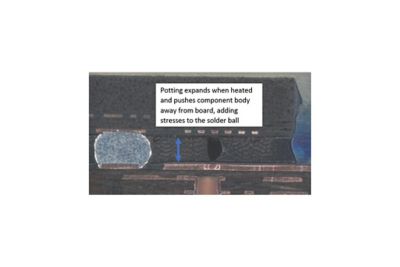
As the potting expands, the solder ball experiences stress.
For example, if an assembly is dip-coated, the coating will flow underneath components like ball grid arrays (BGAs) and quad-flat no-leads (QFNs). The coating will expand during thermal cycling and may “lift” the component off the board, adding tensile stresses to the solder joints.
Certain component mounting conditions and potting/coating application techniques can create unwanted stresses on component solder joints — like tensile stresses. Depending on the material properties of the potting/coating used, these stresses can be large enough to have drastic effects on solder joint fatigue life.
The most important material properties to consider when specifying a potting or coating are the glass transition temperature, modulus and coefficient of thermal expansion — above and below the glass transition temperature. The glass transition temperature refers to the temperature at which a material transitions between a hard/glass-like and soft/rubbery-like consistency.
Learn more about glass transition effect on pottings, coatings and underfill.
One common problem with potting is when an unexpectedly high glass transition temperature is associated with a material that was not fully understood during the product design process. In some polymers used in electronic potting, the elastic modulus can increase by a factor of 20 when the material cools below its glass transition temperature.
If a thermal cycle extends below the glass transition temperature of such a material, the stresses and resulting creep strains experienced by the solder during the cold dwell will be high and damaging. This effect can drastically reduce fatigue lifetime.
The examples mentioned here are just a few of the complex and detrimental loading conditions that can result from not fully understanding the thermal and mechanical material properties of a potting, coating or underfill.
View the webinar below to learn about reliability issues related to pottings and coatings.
Recorded webinar discussing coatings and pottings.
2. Unexpected Temperature Cycling Extremes
Another common cause of unexpected solder joint failure is incorrect characterization of the temperature cycling parameters experienced by the electronic system. For example, on/off cycles, exposure to direct sunlight, travel between different climates and several other sources can add unexpected temperature fluctuations to a printed circuit board assembly (PCBA) or component.
To generate the most accurate reliability metrics of an electronic system, detailed characterization of the temperature cycling it will experience is necessary before running finite element analysis (FEA) simulations or physical product qualifications.
The Ansys Sherlock team has had success generating fatigue life predictions with the Blattau model. The model is a semi-empirical energy-based model that shows fatigue lifetime to be highly dependent on temperature range, dwell time and temperature ramp rate. If the ramps, dwells, maximum temperature and minimum temperature are not fully understood during the design or testing process, key factors that affect the reliability of the product may be overlooked.
Furthermore, if the assembly contains potting or other polymers, the risk of experiencing the glass transition issues, described above, increases if the maximum and minimum temperatures are not accurately determined.
3. Mechanical Overstress Events
Mechanical overstress failures occur when a solder joint experiences excessive loading during a mechanical event — such as a shock, drop, in-circuit testing, board depanelization, connector insertion or PCBA insertion.
Overstress failures can be difficult to prevent because they are often difficult to predict. Shock testing research suggests that the best solution is a random failure distribution of such failures.
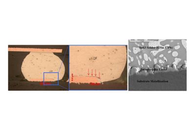
A fracture along the IMC
Solder joint overstress failure typically manifests as a pad crater or a joint fracture along the intermetallic connection (IMC). A pad crater is a crater-shaped crack in the laminate layer beneath the copper pad of a solder joint. The IMC is the region where the copper pad and solder combine to form Cu3Sn or Cu6Sn5. It is the most brittle region of the solder joint, which is why it is the area most susceptible to overstress.
This type of failure is typically seen on finer pitch components — primarily BGAs — or when especially brittle laminates are used. Pad cratering is a serious issue because it often leads to trace fractures. In contrast to fatigue cracks, which typically occur through the bulk of a solder joint, when mechanical overstress failures manifest as joint fractures, they generally occur along the IMC.
Because mechanical event failures can be highly dependent on PCB boundary conditions and geometries, FEA is typically recommended to predict mechanical overstress risk. Complex loading conditions or board shapes are difficult to predict with other methods. Additionally, FEA allows for strain and curvature quantification.
Here is a great resource that discusses how to reduce shock-related failures of electronic assemblies.
Recorded webinar discussing guaranteed reliability
with mechanical shock.
4. PCBA Over-Constraint Conditions
PCBA over-constraint conditions, include:
- Component mirroring
- Board mounting conditions
- Attachment to housings
They are often overlooked design features that can have significant effects on a solder joint’s lifetime.
Mount points, and other board constraints, have a significant impact on the board strain magnitude and location during thermal expansion, mechanical shock events and vibration.
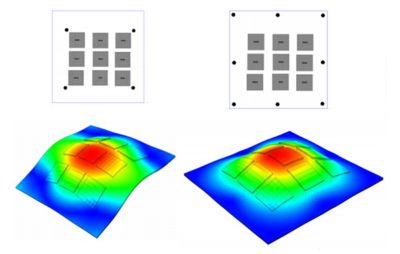
Thermal-mechanical reflection of a circuit under constraints
Constraints reduce board compliance and create board strains that can cause premature solder joint failures on components that are positioned too closely. Additionally, the overall layout of the mount points will directly affect the likely mode shapes of the PCBA.
If these mode shapes are not well understood, the board may be designed in a manner that places sensitive components in regions of high board strain. FEA is a strong mitigation tool to solve this issue because it enables the user to iterate different mounting conditions.
Component mirroring is another common over-constraint condition that can negatively affect solder joint lifetime. Mirroring refers to the position of two components in similar locations on both sides of a PCBA.
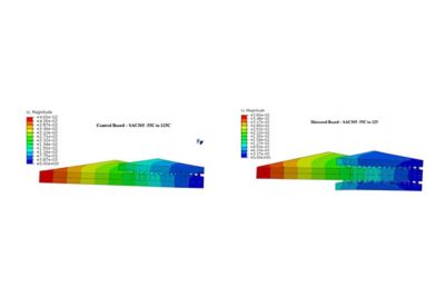
Simulation of a control board and mirrored board
Mirroring reduces the package compliance of the component by constraining board motion, which creates extra stresses in solder joints. Research suggests component mirroring can reduce fatigue lifetime by a factor of 2 or 3.
Here is a great resource that discusses system-level effects on solder joint reliability.
Recorded webinar discussing system level effects on
solder joint reliability.
5. Soldering Defects
All of the mitigation strategies mentioned above will not prevent solder joint reliability issues if the solder joint quality is poor. For this reason, it is imperative to construct PCBAs using a reputable manufacturer with a tightly controlled process.
A wide variety of solder joint defects exists that can negatively affect reliability. Cross sections and visual inspection of solder joints should be conducted before PCBAs reach the field to ensure that manufacturing quality metrics are achieved.
IPC, the Association Connecting Electronics Industries, provides manufacturing standards and acceptability criteria for all types of solder joints. They are typically considered the industry standard for creating high-quality solder joints.
Ansys Sherlock is another useful tool to mitigate solder failure. It is an automated design analysis software solution that offers reliability physics and physics of failure (PoF)-based electronics design. To learn how it can help predict solder fatigue, view the recorded webinar: Introduction to Reliability Physics Analysis.


