-
United States -
United Kingdom -
India -
France -
Deutschland -
Italia -
日本 -
대한민국 -
中国 -
台灣
-
Ansys si impegna a fare in modo che gli studenti di oggi abbiano successo, fornendogli il software gratuito di simulazione ingegneristica.
-
Ansys si impegna a fare in modo che gli studenti di oggi abbiano successo, fornendogli il software gratuito di simulazione ingegneristica.
-
Ansys si impegna a fare in modo che gli studenti di oggi abbiano successo, fornendogli il software gratuito di simulazione ingegneristica.
-
Contattaci -
Opportunità di lavoro -
Studenti e Accademici -
Per Stati Uniti e Canada
+1 844.462.6797
ANSYS BLOG
July 19, 2022
Improve Workflows, Encryption, and Performance with Ansys HFSS 2022 R2
Designers of cutting-edge, high-speed electronics face never-ending pressure to pack more functionality into an ever-shrinking footprint.
The outcome — dense, tightly integrated products — presents significant challenges for signal integrity and electromagnetic interference/compatibility (EMI/EMC) due to the proximity of components, and because of higher data rates and frequencies.
Flexing Your HFSS
A common method for connecting components, printed circuit boards (PCBs), and packages is flex PCB cable technology. This leverages PCB design and manufacturing processes to create economical cabling that can bend and wrap within the design to create connections within a system. For the resulting geometry, it is critically important that an accurate simulation can be achieved to account for any coupling effects under the assembled state.
For years, Ansys HFSS 3D Layout, a full 3D solution for electromagnetic simulation, has enabled accurate modeling and simulation of layered structures. Now, HFSS 3D Layout enables a rigorous workflow for defining and wrapping flex cables for a full HFSS simulation, including coupling effects within the final configured state of the design; no flattened approximation.
From Designs to Ready-to-Simulate Models, Automatically
With HFSS 2022 R2, Ansys is automating the workflow in HFSS 3D Layout and making manipulation easier. The result: a simpler way to generate flex cable meshes and turn original design files into a ready-to-simulate model.
Automation will enable the engineer to bring multiple PCBs in proximity to one another, then grab the flex cables and drop them where they belong. It will even be possible to automate flex cable bending.
Automating the workflow in HFSS 3D Layout will reduce engineering time and effort, translating to lower design process costs overall.
Challenges of Modeling ICs at the Cutting Edge
To protect intellectual property (IP), it is common for integrated circuit (IC) foundries to share only their latest nodes through encrypted technology files. This, of course, presents a problem to physics simulation tools like HFSS, which need the layer dimensions and material properties to extract accurate models and electromagnetic fields from the simulation.
In 2022 R2, a new Encrypted Layout Component feature enables IC designers to work with encrypted technology files in HFSS 3D Layout. HFSS 3D Layout provides a full simulation while obfuscating details like material definitions and layer thickness and still providing the end user with a normalized 3D view of the component. In addition, the resulting design can be encapsulated into an encrypted component file — analogous to HFSS 3D encrypted components of the computer-aided design (CAD).
In short, it’s a win-win for everyone: HFSS now protects IP while enabling engineers to collaborate and design for the tightest possible margins, for the highest possible performance.
HFSS 2022 R2 Performance
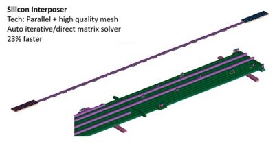
HFSS performance is going up another notch by reducing design and simulation turnaround time. This will benefit all HFFS users, but especially engineers who solve designs at large scale in size and/or complexity.

Among the many improvements to HFSS performance are features such as:
- Parallel mesh refinement technology, which is valuable for IC and interposer designs.
- Reduced adaptive pass memory, enabling larger simulation.
- Improved memory monitoring in a distributed direct matrix solver to deliver more robust simulation performance.
HFSS beta features include:
- Non-uniform memory access (NUMA) optimization for the direct matrix solver to improve scalability with multiprocessor machines.
- Advanced Micro Devices (AMD) math libraries for the direct matrix solver to optimally support the latest AMD processor technologies.
- Distributed mesh fusion solver improvements, which are valuable for high port count models such as 5G mmWave antenna arrays.
Are you ready to create faster and more powerful simulations with the accuracy of HFSS? View our Ansys HFSS 3D Layout Webinar Series. Register today!


