-
United States -
United Kingdom -
India -
France -
Deutschland -
Italia -
日本 -
대한민국 -
中国 -
台灣
-
Ansys si impegna a fare in modo che gli studenti di oggi abbiano successo, fornendogli il software gratuito di simulazione ingegneristica.
-
Ansys si impegna a fare in modo che gli studenti di oggi abbiano successo, fornendogli il software gratuito di simulazione ingegneristica.
-
Ansys si impegna a fare in modo che gli studenti di oggi abbiano successo, fornendogli il software gratuito di simulazione ingegneristica.
-
Contattaci -
Opportunità di lavoro -
Studenti e Accademici -
Per Stati Uniti e Canada
+1 844.462.6797
ANSYS BLOG
June 1, 2023
Analyze Custom ICs Early to Avoid Tapeout Delays
The Ansys acquisition of Diakopto enables semiconductor designers to detect and correct problems earlier
Semiconductor companies are in a constant race to develop next-generation chips with higher speeds, more processing power, more intelligence, and higher precision while condensing them into a much smaller footprint. This poses a big challenge for integrated circuit (IC) designers and layout engineers because what once were minor concerns for electronic design automation (EDA) are now magnified.
Chips aren’t getting smaller because functionality is being removed. Quite the opposite: They’re being condensed while packing more functionality into tiny packages. Those functions are conducted by thousands, millions or, in some cases, billions of wires and transistors that are interconnected in a complex matrix. Such a confined layout causes unintended consequences that limit the performance, reliability, and functionality of designs. The performance of high-speed signals is crucially dependent on the precise characteristics of individual signal wires. The most critical of these are often carefully crafted with custom flows to achieve the best possible performance.

When any issues or performance shortfalls are revealed at signoff — the final design verification before an IC can be “taped out” and sent to manufacturing — it creates considerable delays to go back and rework the design. With today’s complex semiconductors, the verification process can take a considerable amount of time. Before the process can even be restarted, the causes of the issues must be identified and corrected. Finding those root causes can be like finding a needle in a haystack, which further delays development.
Debug Early, Debug Often
To address these concerns, leading electronics companies are doing more analysis earlier in the design process. “Shifting left” in the workflow to find and fix potential challenges early not only enables more efficient performance optimization, but it can also be done more quickly than a rigorous signoff verification. Ideally, this analysis would be intuitive enough to be done by many designers, rather than the relatively few specialists in the workflow, which would further increase efficiency.
This is where Diakopto excels: early analysis, debugging, and optimization of a wide range of high-speed circuits, signal nets, precision analog, and power delivery networks, combined with insights that help users quickly find those proverbial needles in a haystack. The EDA solution provider, founded in 2017, develops products that enable IC design and layout engineers to quickly and easily analyze custom circuits and pinpoint the critical elements that are causing performance bottlenecks. IC system architects can use those findings to optimize and debug designs more efficiently by resolving critical issues caused by layout parasitics.
Layout parasitics are unintended resistance and capacitance (RC) effects that have become more significant in today’s dense, highly complex ICs where unavoidable electrical couplings are more likely. The migration to more advanced silicon process nodes has led to the exponential growth in the magnitude, impact, and number of parasitic elements in modern ICs. Diakopto’s ParagonX helps designers reduce parasitics-related debugging and optimization time from days or weeks to minutes or hours. The ParagonX toolkit is integrated with easy-to-interpret visualization, and offers a comprehensive set of analyses, including resistance and capacitance/coupling analysis; RC delay, AC, and transient simulations; net and device comparison and matching verification; quality assurance and verification; as well as netlist comparison and structural analysis.

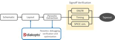
Illustration showing how Diakopto’s technology complements a generic IC design flow by adding analysis for critical circuits like SERDES, data converters, RF, differential circuits, memories, ESD networks, and many more.
Diakopto’s PrimeX enhances existing electromigration/voltage-drop (EM/IR) methodologies by enabling engineers to perform very fast power grid verification, at both the block and top levels. By delivering clear, intuitive results that identify weaknesses and bottlenecks by layer and polygon in the layout, PrimeX helps engineers improve their circuits’ power integrity and reliability while accelerating time-to-market.
Combined Workflow Provides Speed and Accuracy
The company’s products are not intended for signoff-level accuracy, but they’re quick, can be run iteratively many times, and provide actionable analytics to guide designers to optimize their circuit or to fix any problems they uncover. As such, they are a great complement to Ansys Redhawk-SC and Ansys Totem, the industry’s gold standard voltage drop and electromigration multiphysics signoff solutions for digital and mixed-signal designs.
“By joining forces with Ansys, we’re confident that we can solve a broader set of problems in the chip design workflow together, strengthening offerings for our customers and driving more innovations in high-tech designs for data center, 5G, automotive, and mobile applications,” said Maxim Ershov, CEO and CTO at Diakopto in a press release.
We welcome the Diakopto team to Ansys and look forward to adding their EDA expertise to our existing sales, engineering, research, and development teams. Learn more about Diakopto, Ansys Redhawk-SC, and Ansys Totem.


