-
United States -
United Kingdom -
India -
France -
Deutschland -
Italia -
日本 -
대한민국 -
中国 -
台灣
-
Ansys s'engage à préparer les étudiants d'aujourd'hui à la réussite, en leur fournissant gratuitement un logiciel de simulation.
-
Ansys s'engage à préparer les étudiants d'aujourd'hui à la réussite, en leur fournissant gratuitement un logiciel de simulation.
-
Ansys s'engage à préparer les étudiants d'aujourd'hui à la réussite, en leur fournissant gratuitement un logiciel de simulation.
-
Contactez-nous -
Carrières -
Étudiants et universitaires -
-
S'inscrire -
Déconnexion -
Espace client -
Support -
Communautés partenaires -
Contacter le service commercial
Pour les États-Unis et le Canada
+1 844.462.6797
-
ANSYS BLOG
March 14, 2023
Learn How to Combine Multiphysics Analysis and IC Design at SNUG 2023
Ansys is participating in this year’s Synopsys User Group (SNUG) in Silicon Valley on March 29 to present combined electronic design automation (EDA) flows and solution technologies developed through extensive collaboration between the two companies. This strategic partnership is driven by strong demand from our joint customers to address what they consider to be the primary design challenges facing EDA today.
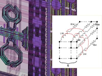
The dominant trend driving the future of EDA design technology is a rapid expansion in the scope of multiphysics that chip designers have to deal with. Detailed analysis of phenomena like thermal analysis, electromagnetic coupling (EMC) and mechanical stress/warpage have been pushed to the forefront of concern by advanced finFET processes and 2.5/3D-IC packaging techniques. Yet many IC design engineers are unfamiliar with these areas of physics where the lines between chip, package, and system design have become very blurred.
These are exciting developments in EDA software that expand the limits of what is possible, but they have also made it very clear that no single company offers all the technology you need to successfully deliver tomorrow’s market-leading products. That is why Ansys — with its deep, decades-long expertise in multiphysics system simulation — is working with Synopsys, an expert in IC design and implementation across multiple technology fronts. The companies have developed joint solutions for our customers in the areas of timing and dynamic voltage drop, 3D-IC thermal analysis, signal integrity, power analysis of emulator activity streams, and high-frequency RF electromagnetic chip design.

SNUG Presentations Address EDA Challenges and Opportunities
Prith Banerjee, Ansys CTO, will present a session on cloud application in EDA: “It’s Cloudy Out There — Is the Ecosystem Ready?” (March 29 at 12:30 p.m.). Prith’s deep expertise in AI/ML will inform his views on Ansys developments in the area of cloud strategy as well as industry and technology trends that are driving real tool applications.
John Lee, VP and GM of the Electronics, Semiconductor, and Optics business unit at Ansys, will be participating in the roundtable discussion panel: “Multi-Die Systems: The Biggest Disruption in Computing for Years” (March 30 at 12 p.m.) with fellow panelists from TSMC, ARM, Mercedes-Benz, and Synopsys. The moderator, Dan Nenni, from SemiWiki, will guide the discussion on this vital topic embraced by leading chip design houses and upending business as usual in EDA.
Ansys will also be joining TSMC, Keysight, and Synopsys in a joint presentation on a combined solution flow for “Accelerating RF/mmWave Design with TSMC Design Reference Flows from Synopsys, Ansys, and Keysight” (March 30 at 10:30 a.m.). The participants will discuss the collaborative solution developed together to provide a comprehensive design flow for radio frequency (RF) millimeter-wave semiconductors on TSMC N6RF and N16FFC technologies.
Ansys will also be demonstrating some of the latest advances in hardware security when Ansys’ Dr. Lang Lin will be joined by Dr. Nitin Pundir from IBM to discuss “Pre-Silicon Laser Fault Injection Assessment Methodology” (March 30 at 2:15 p.m.). The presentation will cover how to make designs more secure against laser side-channel attacks before the manufacturing stage, when it is still possible to close any vulnerabilities.
Join us at SNUG 2023
Make sure to register for SNUG and stop by the Ansys table in the exhibit hall for more information on the many areas of technical collaboration between Synopsys and Ansys.


