-
United States -
United Kingdom -
India -
France -
Deutschland -
Italia -
日本 -
대한민국 -
中国 -
台灣
-
Ansys s'engage à préparer les étudiants d'aujourd'hui à la réussite, en leur fournissant gratuitement un logiciel de simulation.
-
Ansys s'engage à préparer les étudiants d'aujourd'hui à la réussite, en leur fournissant gratuitement un logiciel de simulation.
-
Ansys s'engage à préparer les étudiants d'aujourd'hui à la réussite, en leur fournissant gratuitement un logiciel de simulation.
-
Contactez-nous -
Carrières -
Étudiants et universitaires -
-
S'inscrire -
Déconnexion -
Espace client -
Support -
Communautés partenaires -
Contacter le service commercial
Pour les États-Unis et le Canada
+1 844.462.6797
-
ANSYS BLOG
May 16, 2023
Low-Power IC Design: Techniques and Best Practices
Low-power IC (integrated circuit) design is a crucial aspect of modern electronics, as it allows for longer battery life and lower energy consumption in devices. The growing market for battery-powered devices has made it necessary for chip designers to strongly consider different techniques for reducing the power consumption of ICs. There are several techniques that can be used to reduce the static and dynamic power consumption of ICs. DC current and leakage current are the source of static power, whereas dynamic power is frequency dependent, which comes from transistor switching and short circuit power.

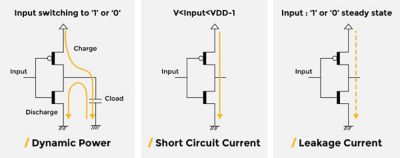
Figure 1. Components of power in complementary metal-oxide-semiconductor (CMOS) circuit
To create a low-power design, the designer must reduce every individual component of power that is contributing to the overall power consumption. Figure 1 shows both dynamic and static power characteristics. The dynamic charging of complementary metal-oxide-semiconductor (CMOS) inverters makes power consumption directly proportional to the clocking frequency. Power leakage through transistors during no activity constitutes static power.
The low-power designer can reduce the total power consumption by controlling the supply voltage, reducing circuit complexity and clocking frequency, and monitoring DC current sources and the capacitance of switching nodes. Everything is connected, so the designer must trade off between these factors by testing and using low-power design techniques to optimize the performance of the design.
Techniques and Best Practices for Low-Power Design
Clock Gating
One way of reducing the power consumption of a device is to tweak the design at the register-transfer (RTL) level. It is one of the most common techniques for reducing dynamic power consumption. At the RTL level, power is consumed either when the transistor is changing its logical state or when the power is used to charge the load capacitance. The total dynamic power is:
Pdynamic = Pcap + Ptransient = (CL + C) Vdd 2 f N3
in which CL is the load capacitance, C is the internal capacitance of the chip, f is the frequency of operation, and N is the number of bits that are switching. It’s easy to reduce the dynamic current flow by gating the clock when not required. Instead of using AND/NOR gates, it’s better to use latch-based clock gating to avoid any additional power consumption. Turning off the clock signals to certain parts of the IC can greatly reduce power consumption, as the transistors in those areas will not be switching and consuming power.
Power Gating
All blocks are not operational all the time in an IC; it depends on their application in the device. There is no need to supply power to a block if it is not functional in a particular instance. By turning off the power supply to non-functional blocks, power consumption can be reduced. To efficiently use this technique designers can use isolation blocks to prevent unnecessary signals coming from power-gated blocks.
Frequency Gating
As we know, chips consist of multiple blocks, and each block does not require the highest possible frequency to operate. The best technique can be to segregate the blocks based on their frequency requirement and provide a different clock signal to a different block. This method can greatly reduce the localized dynamic power consumption of the IC.
Multivoltage Design
No block in the design requires the same amount of power to operate. You can partition the chip depending on the performance of the block and its voltage requirements. The higher the voltage requirement, the higher the consumption. By creating voltage islands with different voltage inputs, it’s easy to reduce the overall power consumption of an IC.
Dynamic Voltage and Frequency Scaling
There is a limitation to the voltage island technique — once the voltage supply to a block is designed it cannot be changed later. The dynamic voltage scaling technique gives the flexibility to the designer to change the voltage later as per the requirement. The designer can program the regulator which changes the power supply to various blocks according to the varying current. Similarly, voltage scaling can be combined with frequency scaling which enables the designer to modify clock signals supplied to each block with the help of a software program.
Power Reduction
The most important power reduction technique by far is to lower the supply voltage of the chip. Dynamic switching power is dominant for finFET designs and is proportional to the square of the supply voltage, hence the intense drive towards ultra-low-voltage (ULV) processes.
Leakage Power Trade-Off
Leakage power is an important power drain in pre-finFET technologies and is best controlled with multi-Vt libraries. These libraries offer two or three versions of every cell, each one with a different performance/leakage trade-off. This lets designers use fast, leaky cells in timing critical paths and use slower, low-leakage cells in less critical paths.
Overall, there are many techniques that can be used to reduce the power consumption of ICs. By implementing these techniques and using appropriate design and simulation tools designers can overcome these challenges. Tools such as Ansys RedHawk-SC enable engineers to simulate and predict design behavior at every design stage, which allows you to design low-power ICs that are more energy-efficient and have longer battery life.
Low-Power Design Challenges
- Voltage drop margins become very tight, especially with ultra-low voltage designs. This evolution has made voltage (IR) drop signoff validation an essential part of all modern IC design.
- Low supply voltages make path timing much more susceptible to dynamic voltage drop (DVD). Also, it is very challenging to analyze DVD with sufficient coverage to catch all possible switching scenarios. Careful voltage drop analysis is crucial to minimize the impact of DVD on timing and avoid frequency loss due to unexpected IR drop impacts.
- Multivoltage regions require careful management to ensure the proper signal transitions and signal integrity between different voltage regions. UPF is a standard designed to help address this challenge.
- Power gating introduces challenging transition phenomena — both electrical and logical — when switching a block back on again.
- Clock gating is most effective when implemented as close to the root of a clock distribution network as possible, but that is limited by the feasibility of the enable signal timing if it can arrive on time. This leads to trade-offs that balance achieved power efficiency against design optimization effort.
The validity of any power analysis is critically dependent on the circuit activity. Yet it is not simple to generate a realistic and representative activity scenario that captures the full range of possible power regimes in real-life usage across all modes. A common mistake is to use functional verification activity vectors to calculate power; these are misleading and irrelevant for power analysis. Good activity vectors can be generated by hand, automatically by the power tool ("vectorless"), or by hardware emulators running real applications.
Redhawk-SC is a software tool that is widely used for power analysis in IC design. It addresses this issue by providing a comprehensive set of capabilities for accurately predicting and analyzing voltage drops in the chip. RedHawk-SC uses sophisticated algorithms to model the behavior of the chip's power delivery network, considering factors such as on-chip resistance, capacitance, and inductance. This allows IC designers to identify potential voltage drop hot spots and simulate the behavior of the chip under various operating conditions. For designing low-power ICs, designers must consider all the aspects of the power supply delivery network and predict the voltage behavior while designing.
For more, visit the home of Ansys RedHawk-SC or read "Foundations of Semiconductor Power Integrity Analysis and Simulation."


