TOPIC DETAILS
What is Signal Integrity?
A system's signal integrity (SI) is a measure of how much an electrical signal changes between entering and exiting a circuit. For digital electronics, that signal is an electric current in which voltage varies between a high and a low value over time.
Signal integrity is fundamental to any modern electronic system. The industry uses the term “integrity” as it means adhering to a code, remaining unimpaired, and being complete and undivided. If the waveform of the signal varies significantly from the original because of crosstalk, impedance mismatch, and losses, the receiver will not be able to read the signal, creating a signal integrity issue. That is why signal integrity engineering — analyzing and improving signal integrity issues — is an important part of designing integrated circuits (ICs), IC packages, and printed circuit boards (PCBs).
The increase in signal speed and decrease in the size of PCBs and packages make handling signal integrity issues even more challenging. High-speed digital signals and smaller geometry make signal noise and distortion more pronounced. However, as the challenges have grown, so has the industry's understanding of how to deal with them, along with the capability of the tools engineers can use to define, simulate, and adjust their electronic systems.
Distortion of that waveform, noise, shifting in time, and decreases in amplitude occur as the electrons flow from the driver to the receiver because of resistance in the material, the electromagnetic field created from the moving electrons, current induced from other electromagnetic fields, and the capacitance of the circuit. In a PCB, materials, the shape of the traces that create the circuit, the placement and thickness of various layers, and how current is transmitted between layers drive these effects.
It’s also important to mention the closely related issues classified under power integrity. While signal integrity deals with the fidelity of the signal in a PCB, power integrity deals with the quality of the power delivered to the components that will send and receive those signals. The same issues of impedance, inductance, and attenuation that impact signal integrity play a role in power integrity. Also, changes to one may negatively impact the other, so engineers need to simulate and measure both when improving a design.
Why is Signal Integrity Important?
If signal integrity is not addressed, digital devices can have significant problems. The most significant issue arises when a signal distorts so much that the 0 or 1 transmitted across a circuit is not received correctly, and the binary value is wrong. Also, the device may fail when the noise or time lag is significant. In today’s highly complex PCBs, with hundreds of PCB traces, it only takes one signal path with signal integrity issues to make the whole board unusable.
The realities of physics make it impossible to send a signal through a circuit without some change in the signal by the time it gets to the other end. With a strong understanding of single integrity analysis basics, a grasp on how SI impacts modern circuit design, and methods to identify and deal with signal integrity issues, design teams can minimize the integrity of the signals across their devices and push to ever smaller form factors and higher frequencies.
The Basics of Signal Integrity Analysis
The physics around electrons moving through materials compromises a signal's integrity. Maxwell’s equations capture the relationship between charge and current, how current creates electromagnetic fields, and how fields change current.
In short, the interconnects in a PCB, called transmission lines for digital signals, act like antennas, resistors, and capacitors. The signal’s characteristics, the material properties of conducting and dielectric materials, geometry, and the relative position of the circuits and layers in the PCB determine the magnitude and impact of the physics described in Maxwell’s equations.
The 4 Types of Signal Integrity Problems
The basic physics mentioned above drive signal integrity issues into one of four categories:
1. Electromagnetic interference (EMI)/electromagnetic compatibility (EMC)
In any high-frequency circuit, the right combination of geometry and frequency turns a trace or a via into an antenna broadcasting a signal that can couple with other circuits on the same PCB or in other devices, connectors, or cables in the same or nearby devices. When another circuit receives interference, the energy in the electromagnetic field can induce a current, creating noise in that signal. Broadcasting electromagnetic waves also reduces the signal's voltage because creating the field consumes power. Designers must minimize the interference (EMI) and also ensure that the device they are developing is compatible with the electromagnetic environment (EMC) it operates in.
2. Crosstalk
Crosstalk is another form of electromagnetic interaction. It occurs when the signal in high-speed traces near one another couple their electric and magnetic fields. The unwanted signal originates from what is called an aggressor trace that couples with the signal on a neighboring transmission line, called a victim trace. The types of coupling are:
- Capacitive coupling: caused by the electrical field of the aggressor circuit inducing a voltage in the victim circuit
- Inductive coupling: caused by the magnetic field of the aggressor circuit inducing a voltage in the victim circuit
- Conductive coupling: Caused by the current of both signals coupling on the return path in the ground plane
3. Simultaneous switching noise (SSN)-caused ground bounce
Ground bounce happens when the signal ground of a PCB is not the same at all points. It is a signal integrity problem caused by multiple circuits changing their voltage between the high or low state at the same time, inducing a voltage increase in the ground plane. This causes the low-state voltage, the 0 in a binary signal, to be higher than expected. Sometimes, the bounce is high enough to cause a reading of a false high state.
4. Impedance mismatch
Designers need to consider the impedance of an alternating current (AC) circuit. Impedance is the resistance to current flow and changes to current caused by inductance and capacitance. An impedance mismatch occurs when the impedance changes somewhere along the circuit. The mismatch causes a portion of the signal to reflect back and then propagate back and forth until attenuated. Besides adding noise to the signal, impedance mismatch can cause uncertainty in timing, which is called jitter. A standard tool to evaluate impedance mismatch is time-domain reflectometry (TDR). TDR measures the reflection in a transmission line.
Visualizing Signal Integrity With an Eye Diagram Analysis
Eye diagram analysis is one of the most common tools used in exploring signal integrity. An eye diagram, also called an eye pattern, is a way to view the response of a digital circuit over time. A repeating signal is input into the analyzed circuit, and the output signal is measured over time. Each bit of data is folded on top of the other, with time on the X-axis and amplitude on the Y-axis. Since the input signal is a square wave, a perfect circuit would produce an image showing two horizontal lines on the top and bottom and two vertical lines in the middle, separated horizontally by the length of one bit of data and vertically by the voltage difference in the signal.
But no circuit is perfect, so the shape transforms into something that looks like an eye. The signal integrity issues discussed above show up as distortion from straight lines. The figure below shows the typical values that reveal problems in a circuit. Values like rise time, fall time, jitter, and eye-crossing percentage reveal how the signal distorts and what noise that gets into the system does to the signal.
By comparing eye diagrams before and after a change to routing, geometry, or material, designers can see how those changes improve the signal integrity of a circuit.
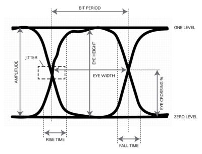
This analytical approach was originally developed to quickly visualize a circuit's signal integrity with an oscilloscope. Today, engineers use eye diagrams to examine circuitry's performance as predicted in a simulation. This allows designers to explore changes quickly and see the impact long before a PCB is prototyped.
Signal Integrity and Integrated Circuits (ICs)
This article focuses on SI in PCBs, but signal integrity in IC chips is also key. Because the feature sizes are smaller and the data rates are even higher, signal integrity is an even more important consideration when laying out integrated circuits and defining interconnects. Coupling effects from switching of other signals are the biggest driver of SI problems in chips. Also, just outside the chip, the wires that serve as interconnects to the package are close enough to suffer from significant crosstalk.
Prototyping an IC chip is very difficult, so signal integrity and power integrity are modeled using simulation as early as possible in the design process to identify and rectify potential problems. Chips are verified with these tools to see if they will perform as expected before starting the manufacturing process.
Tips for Identifying Signal Integrity Issues and Improving Performance
The most important step engineers can take to avoid SI issues in high-speed digital designs is to follow the well-established industry design rules for PCB design. Some typical rules include:
- Specifying the distance between traces
- Avoiding abrupt changes in trace width
- Staying within allowable corner radii
- Avoiding trace and via stubs
- Not placing discontinuities in the ground layer that interrupt the return path
- Designing differential pairs to have the same length
- Decrease the impedance of the power plane
- Strategic placement of ground planes and proper thickness of each layer in the PCB
- Avoiding vias for higher frequencies
Even if designers follow all the design rules for their PCB layouts, problems can still occur. Challenges also arise when balancing multiple rules, manufacturing constraints, size limitations, and cost concerns. Simulation is usually deployed to identify these issues and make improvements.
With a good parametric design and a robust simulation toolset like Ansys SIwave™ PCB and package electromagnetics simulation software and Ansys HFSS™ 3D high-frequency simulation software, engineers can quickly conduct trade studies to explore solutions.
Because an electromagnetic field or current in a trace cannot be seen, heard, or felt, engineers employ simulation to visualize the fields and fluxes that occur. This visualization allows engineers to view the propagation of electromagnetic fields, see the signal return path, visualize heating in the PCB and under components, and look at the crosstalk between trace pairs.
The Future of Signal Integrity
The future of SI is similar to its recent past — increasing data rates, rising clock speeds, and growing bandwidth requirements. Packaging demands also drive systems to use smaller PCBs, pack more components on those PCBs, and bend them into convoluted shapes with flexible PCBs . To meet industry demands and grow market share, companies will introduce new manufacturing processes and experiment with different materials. Both will impact signal integrity.
Another trend that will accelerate in the near future is tighter integration between layout and simulation, bringing more physics up front in the design process. While creating a strategy for a PCB, engineers will be able to explore the electromagnetic fields, power integrity, thermal characteristics, and mechanical robustness of their designs.
Like everything else, artificial intelligence (AI) will play a role in the future of minimizing signal integrity problems. Many layout tools already use older forms of AI to enforce design rules to route traces when converting schematics into PCB layouts. The new generation of generative AI tools will drastically improve the capabilities of both design and simulation tools.
