


TOPIC DETAILS
What is a Printed Circuit Board (PCB)?
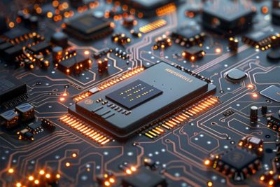
A printed circuit board (PCB) is a mechanical base used to hold and connect the components of an electric circuit. PCBs are used in nearly all modern consumer electronic devices and accessories, including phones, tablets, smartwatches, wireless chargers, and power supplies These multi-material, multilayer boards form the stable foundation of a PCB assembly (PCBA) and are responsible for directing current flow between both active and passive components.
Active Components: Generate energy | Passive Components: Store energy |
|---|---|
| Transistors | Resistors |
| Diodes | Capacitors |
| Integrated Circuits | Inductors |
| Amplifiers | Transformers |
| Sensors | Relays |
| Crystal Oscillators | Fuses |
The base layer of a PCB is typically made from a combination of strong, nonconductive materials that provides insulation, water resistance, and temperature stability. Common PCB materials include FR4, metals, and polyimide (PI). Cost savings, functional performance (such as thermal expansion), and eco-friendliness are all factors for consideration when choosing materials for a PCB.
Etched onto the base layer of a PCB are pathways that carry signals from point to point. Called “traces,” these thin bodies are usually made of copper, a highly conductive material that allows electrons to move with little resistance between components.
Types of PCBs
Different types of PCBs offer different performance qualities and are often classified based on the malleability of the substrate used. These substrates can be rigid, flexible, or a combination of both.
| Rigid PCBs | Flexible PCBs | Rigid-Flex PCBs | |
|---|---|---|---|
| Materials | Fiberglass or metal | Polyimide film | Both bendable and solid layers |
| Benefits | Cost effective and easy to mass produce | Lightweight and bendable | Durable and space efficient |
| Application Examples | Computers, vehicles, electronics, home appliances, industrial equipment, electric tools | Laptops, tablets, phones, cameras, medical devices, vehicle electronics, displays | Radar equipment, avionics, LCD displays |
In addition to these three main types, PCBs can also be categorized using other criteria, such as component placement (single-sided or double-sided PCBs), material (metal-core or ceramic PCBs), connection density (high-density interconnect and ultra-high-density interconnect PCBs), or number of layers (16-layer PCB).
Rigid PCBs are the most widely used type of printed circuit board.
PCB Applications by Industry
If it has an on switch, chances are good that it has a PCB. Used in nearly every electronic device, PCB usage spans industries and device types.
Hi-tech: Custom PCBs power innovation in the highly complex and fast-paced hi-tech industry, including 5G infrastructure and high-speed data processing. These boards can feature high layer counts and unique materials as this industry is on the cutting edge of device development.
Aerospace and Defense: Reliability is key in these applications, in which devices are often remote and can experience extreme environmental considerations (such as temperature, vibration, or shock). Here, PCBs are used in sensors, power supplies, and navigation systems for satellites and aircraft.
Automotive: While PCBs can be found throughout all modern vehicles in heads-up displays, airbags, advanced driver-assistance systems and more, they have a particularly critical role in electric vehicles, as they manage electric motor operation and power delivery.
Energy: PCBs are essential to the generation, collection, and distribution of power. Their reliability keeps the energy sector up and running while facilitating communication between the power grid and controllers, energy storage, and systems monitoring.
Industrial: The automated equipment used in industrial applications relies on PCBs to stand up to intense conditions including high voltage currents, machinery vibration, and extreme temperatures. They can be found in manufacturing drills and presses, measuring equipment, and high-speed video capture.
The Basics of PCB Design
Early circuit board designs relied on through-hole construction, followed by surface mount technology (SMT). For decades, designs were drawn by hand, making manufacturing slow and expensive. With the introduction of computers, the entire design process changed, accelerating production while also improving consistency and functionality. Today’s manufacturers use simulation software for PCB design to model, analyze, and validate their designs at every step of development.
The challenges of PCB design include size constraints, thermal considerations, electromigration, mechanical integration, and power efficiency. These complexities require designers to work with a diverse set of experts to ensure electrical, mechanical, and thermal engineering considerations are addressed throughout the process.
The PCB Design Process:
- Schematic creation: Designers draw a 2D blueprint of the PCB using electronic computer-aided design (ECAD) software. This identifies the PCB’s components, their placement, and how they will be connected.
- Material selection: Based on the needs of the final assembly, designers choose materials to be used on the board. These choices can include FR-4, polyimide laminates, composite epoxy materials (CEM), liquid crystal polymer, and more.
- Design review: Before production, simulation software is used to test and validate how the board will perform under various circumstances. These tests ensure the component arrangement will achieve all requirements.
How Are PCBs Manufactured?
Once this process is complete, the board is ready to be fabricated. PCB manufacturing is a multistage process with many critical phases, but the key steps include printing, etching, pressing, drilling, silk screening, and masking.
- First, the PCB schematic is printed onto a copper-clad substrate.
- Then, the excess copper is removed in a process called etching to reveal the traces and pads for the circuitry.
- Next, alternating layers of materials are pressed together using high heat, and the board is drilled for mounting holes, through-hole pins, and vias.
- A silkscreen layer is then added to mark the surface with information like polarity, names of connectors, and company logos.
- Finally, a solder mask is applied to protect against oxidation and solder bridge formation.
The Future of PCBs
As the backbone of modern electronics, PCBs will continue to evolve as the devices and machines they power continue to get smaller, more flexible, and more powerful. Miniaturization, along with transparent and stretchable materials, will allow PCBs to complement electronics designs in numerous interesting ways. And as electrification drives innovation in automotive and aerospace, PCBs will play a large role in defining how cleaner energy can fuel systems such as communication and navigation.
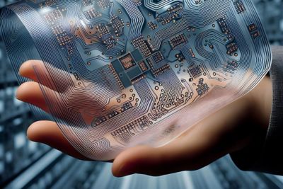
Transparent PCBs are made with ceramic or glass to facilitate see-through devices.
Learn more about Ansys Maxwell software’s new capability for flex and rigid PCB design, and find more information on Ansys Sherlock electronics reliability solutions.