


In semiconductor design, parasitics are the unintended electrical effects and interactions caused by the interconnect wires. Parasitics alter the behavior of a circuit in complex ways, and their impact has grown from an afterthought to a first-order effect. Analysis and debug of analog interconnect parasitics too often rely on a patchwork of vendors and point tools that fail to address the growing complexity of multiphysics requirements with any clear strategy.
Analog integrated circuits (ICs), or chips, have been around since the dawn of the semiconductor age and analog engineers have grown to rely on a design methodology and ecosystem that are quite distinct from that of the larger, more glamorous digital chips. But in the past few years there has been a significant surge in demand for analog design driven by powerful market trends like the pervasive adoption of wireless connectivity, electric vehicles, high-speed digital connectivity in data centers, and multi-die 3D-ICs. This has caused leading design companies to focus on creating more efficient and capable analog design flows to remain competitive and take advantage of this market opportunity.
Analog Design Trends and Challenges
Unlike the digital IC world, analog designers have mostly not chased after the latest and greatest silicon process technologies, which are optimized for large, high-density digital designs. In fact, analog designers are more comfortable working with mature, trailing processes that offer more control over signal quality in their typically smaller, higher-speed circuits. However, the surge in analog design has come with a set of challenges.
- Signal speeds continue to increase to the point where they require more accurate and more comprehensive electromagnetic analysis, even for nominally digital communication channels like a serializer/deserializer (SerDes).
- The analog portions of a system-on-chip (SoC) are forced to use the same advanced silicon process as the rest of the mainly digital chip and so must deal with the intricate silicon effects that complicate design at these advanced nodes.
- The sheer size of analog designs is growing as customers demand more capable solutions. This is straining the capacity of traditional analog design tools, especially for circuits like memories, phased array radar, 3D-IC interposers, and image sensors.
These technical challenges all contribute to the biggest challenge of all: designer productivity. The delivery schedule and design cost of an analog chip is largely determined by the number of engineering hours it absorbs. An analog engineer’s time is dominated by circuit analysis and debug. It’s reported that 35% to 50% of the total project time can be consumed by these activities – and in some cases much more. Debugging is often unpredictable and can be quite time-consuming because it involves multiple simulation runs and the use of various extraction and analysis tools to understand what’s happening with the design. Particularly for advanced silicon processes, the layout parasitics have become a first-order effect – sometimes even dominating the behavior of the active devices (transistors). Interconnect effects and parasitics have become central to both circuit behavior and total design cost.
The reasons for their increased impact are the ever-larger parasitic resistance and capacitance (RC) values and the growing number of parasitic elements. This leads to longer simulation times and complex, non-linear interactions that are often counter-intuitive and difficult for designers to understand and debug.
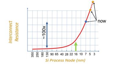
Parasitic resistance increases exponentially in more advanced silicon processes. This is one factor making parasitics a first-order effect in modern analog design.
It stands to reason that successful analog design teams need to have a well-thought-out strategy for dealing with the many multiphysics effects caused by layout interconnect. Not only for today’s issues, but also a strategy for future requirements that will inevitably be even more complex, possibly involving new materials like silicon carbide (SiC), or new physics like photonics.
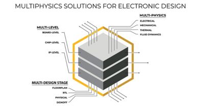
Today, many design houses have a fragmented approach to interconnect analysis with many different vendors that reflect how point-solutions were added over time to plug holes in the design flow. We believe it is time to stand back and approach the interconnect multiphysics domain as a distinct area of expertise that calls for the same strategic approach used to select layout platforms or simulation software.
A Strategic Solution for Interconnect Multiphysics
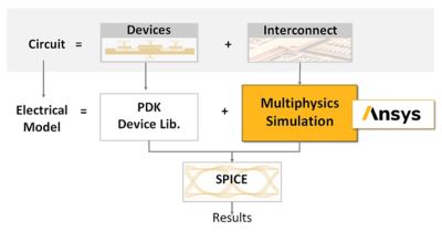
They say you can’t fix what you can’t measure. The electrical models for active devices in a process design kit (PDK) are created with a dedicated suite of library characterization tools and captured in a library for easy reuse. But this doesn’t work for interconnect parasitics: every layout must be extracted from scratch, for every design iteration as shown in the figure below. That is why analog design engineers devote so much time and effort to interconnect analysis. Ansys has recognized the importance of interconnect analysis as a distinct design issue and offers design teams a consolidated, strategic solution.
Ansys provides a comprehensive, strategic solution to the growing productivity and accuracy challenge of analyzing and debugging parasitic interactions for high-speed designs, advanced process nodes, and very large analog circuits.
Ansys offers a broad array of proven and foundry-certified multiphysics solutions to cover all interconnect effects on semiconductors targeted at giving designers a full spectrum of design insights with root-cause analyses of parasitic interactions. This integrated multiphysics approach ensures high-accuracy-proven engines for better results and high-efficiency debugging to save time. Ansys’ long track-record of success in multi-scale solutions also allows these same chip multiphysics tools to extend to the package, PCB, 3D-IC, and product levels.
The interconnect multiphysics covered by Ansys solutions include products and platforms for all the following areas of concern to analog and mixed signal designers:
- RC parasitics: Sophisticated and high-capacity resistance and capacitance parasitic analysis that can identify root causes in minutes to drastically reduce debugging times, especially for analysis of the top hierarchy level.
- High-frequency electromagnetics: Vital to any high-speed design like radio frequency (RF), millimeter-wave, 5G, Wi-Fi, SerDes, physical layer interconnects (PHY), and analog-digital converters (ADC/DAC) is the modeling of all the coupling fields between wires. A special application of high-speed interconnects are inductors and transmission-lines that call for specific design and analysis features.
- Thermal: Integrated thermal engines proven over many years deploy AI-driven meshing combined with industry-leading voltage-drop analysis to identify layer-by-layer temperature maps for semiconductor devices, including local Joule self-heating, transient thermals, system-level cooling, and ambient heat.
- Thermo-mechanical: Mechanical stress and warpage are a consequence of temperature gradients and material mismatches. These mechanical issues not only compromise product reliability but can also cause stress-induced electrical changes.
- Voltage drop and electromigration (EM/IR): Considered by foundries to be a signoff requirement, voltage-drop analysis tools identify both static and dynamic power loss in both supply wires and analog signal wires. And electromigration analysis is an essential component of long-term product reliability.
- Power device analysis (RDS-ON): The parasitic elements within high-power devices and switches must be modeled with maximum accuracy in the design stage to avoid power loss and over-heating of the device.
- Photonics: The growing popularity of co-packaged optics for faster data rates has introduced many design teams to the new physics around optical electronics — including thermal stabilization and mechanical stress minimization.
- Signal integrity: Interposer interconnect and die-to-die signal paths on 3D-ICs, like high-bandwidth memory (HBM) interfaces, demand specialized signal integrity analysis to accurately model the entire communication channel.
- Electrostatic discharge (ESD): Protection circuits that prevent damage due to electrical overstress are analog elements on every chip. Traditional analysis at the very final signoff stage has become a bottleneck as designs get bigger and the industry adopts multi-die design. New methodologies allow significantly faster ESD analysis earlier in the design flow.
- Substrate noise: Noise injection into the silicon substrate is particularly important for sensitive analog designs and calls for comprehensive modeling of the noise sources and the distribution physics.
- Antenna design: Efficient beamforming for radio and radar relies on high-accuracy modeling of the propagation through free-space and interactions with material objects surrounding the antennas.

Parasitic interconnect effects have a huge impact on circuit behavior and are increasingly multiphysics-driven and intertwined. A piecemeal approach to addressing these challenges reduces engineering efficiency, increases design costs, and limits design optimization. The interconnect analysis market should be approached with the same strategic mindset as other critical design sectors to not only increase efficiency today but also future proof your design flow for the new requirements that you will face as technology demands accelerate.