Metal–oxide–semiconductor field-effect transistor (MOSFET) gate resistance is an extremely important parameter, especially in high frequency, advanced semiconductor nodes (16 nm and smaller). Gate resistance determines many characteristics of MOSFETs and complementary metal–oxide–semiconductor (CMOS) circuits, such as:
- Switching speed
- RC (resistor-capacitor) delay
- Fmax — maximum frequency of oscillations
- Gate (thermal) noise
- Series resistance and quality factor in MOS capacitors and varactors (voltage-controlled capacitors)
- Switching speed and uniformity in power field-effect transistors (FETs)
But determining the actual magnitude of gate resistance is difficult for these nodes because of parasitic resistance, capacitance, and inductance, among other complications. Parasitic effects are the unwanted resistance, capacitance, or inductance effects that exist in a circuit design due to physical imperfections in the layout and materials of the design. Parasitics, as they are called, can cause power loss and heating; they also degrade signal quality. To better understand the operation of a gate, it is important to extract these parasitic effects from the model to obtain the real values of resistance, capacitance, and inductance.
Specialized electronic design automation (EDA) tools such as Ansys ParagonX integrated circuit layout parasitics analysis and debugging software can be used to analyze gate resistance by visualizing resistor-capacitor (RC) network connectivity for post-layout netlists, including SPEF (Standard Parasitic Exchange Format, an IEEE standard) and DSPF (Detailed Standard Parasitic Format). These tools can probe the netlists to see and inspect R and C values and perform other electrical analyses. SPICE models can also be useful, although parasitic extraction is considered a more accurate method of calculating parasitic R and C values around the devices, since it "knows" about the layout.
Many papers have been written about gate resistance. However, for the practical work of IC designers and layout engineers, some important things have not been discussed or explained:
- How do parasitic extraction tools handle gate resistance?
- How can you evaluate gate resistance from the layout or from an extracted, post-layout netlist?
- How can you identify if gate resistance is limited by the "intrinsic" gate resistance (gate poly) or by gate metallization routing, and what are the most critical layers and polygons?
- Is the gate distributed effect (factors of 1/3 and 1/12 for single- and double-contacted poly, respectively) captured in IC design flow in the process design kit (PDK)?
- Is the vertical gate resistance component captured in foundry PDKs?
- Should the gate be made wider or narrower to reduce gate resistance?
Here, we will try to shed some light on these under-discussed issues and provide insights for IC design and layout engineers to better understand gate resistance in their designs.
Gate Resistance Definition and Measurement
Gate resistance is an "effective" resistance from the driving point (i.e., gate port or gate driver) to MOSFET gate instance pin(s), as shown in Figure 1. An instance pin is a connection point between a terminal of a SPICE model and a resistive network.

Figure 1. MOSFET cross-section and schematic illustration of gate resistance
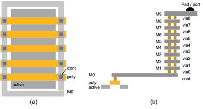
However, the simplicity of the schematic in Figure 1 may be misleading. Gate nets can be very large and contain many driving points, dozens of layers (metal and vias), millions of polygons, and up to millions of gate instance pins, as shown in Figure 2.

Figure 2. Schematic illustration of the top view and cross-sectional view of MOSFET gate network
A gate network is a large distributed system with one or several driving points and many destination points. It looks and behaves like a huge, regular clock network, distributing the gate voltage to an FET. Deriving an equivalent, effective gate resistance for such a large and complex system is not a simple and straightforward task. SPICE circuit simulation does not explicitly report gate resistance values, meaning parasitic extraction tools are needed.
Gate Resistance Handling by Parasitic Extraction Tools
All industry-standard parasitic extraction tools handle gate resistance and its extraction similarly. In layout, the MOS gate structure is represented by a 2D mask traditionally called "poly" (polysilicon), even though the material can be formed by a complex gate metal stack and may have a complex 3D structure.
The extraction tools essentially break the poly line at the intersection with the active (diffusion) layer (the dark gray shaded area in Figure 3). This yields two sections for analysis: "gate poly" (poly in the active region; the yellow shaded area) and "field poly" (poly outside the active region; the light gray shaded area). Together, the poly plus active regions constitute a transistor.

Figure 3. R and RC extraction around a MOSFET gate
The gate poly (yellow shaded area) is also fractured at the center point, and a gate instance pin of the MOSFET (SPICE model) is connected to the center point of the gate poly (the black vertical line in the center of the yellow shaded area). The gate poly is represented by two parasitic resistors connecting the fracture points. Parasitic resistors representing the field poly are connected to the gate contacts or to MEOL (middle-end-of-line, consisting of interconnect metal/via) layers and further to upper metal layers.
MOSFET extrinsic parasitic capacitance between gate poly and source/drain diffusion and contacts is calculated by parasitic extraction tools and assigned to the nodes of the resistive networks. The details of the parasitic capacitance connection to the gate resistor network may have a large, significant impact on transient and AC response, especially in advanced nodes where gate parasitic resistance is huge.
These details can be seen in the DSPF file, but they are not usually discussed in the open literature or foundry PDK documentation. Visual inspection of text DSPF files is tedious and requires expertise. Simulation software like the ParagonX application can be used to visualize RC network connectivity for post-layout netlists (e.g., DSPF, SPEF), inspect R and C values, perform electrical analysis, and do other useful things.
A Reduced-order Gate Model
A MOSFET gate forms a large, distributed RC network along the gate width, as shown in Figure 4.

Figure 4. Distributed properties and model of the gate along the gate width
This distributed network has a different AC and transient response than a simple lumped one-R and one-C circuit. Researchers showed that an RC network such as this behaves approximately the same as a network with one R and one C element,1 where:
- C is the total capacitance
- R=1/3 * W/L * rsh for single-sided connected poly
- R=1/12 * W/L * rsh for double-sided connected poly
Here, W is the width, L is the length, and rsh is the sheet resistance of the poly. The coefficients — 1/3 and 1/12 — effectively enable an accurate reduced-order model for the gate, reducing a large number of R and C elements to two (or three) resistors and one capacitor. Using a reduced-order model simplifies and accelerates the calculations done by the parasitic extraction software.
Impact of Interconnect Parasitics on Gate Resistance
In older node technologies, metal interconnects such as metal and vias had a very low resistance, and gate resistance was dominated by the gate poly. The analysis and calculation of gate resistance was very simple.
When technologies reach 16 nm and smaller, interconnects have very high resistance and can contribute significantly (50% or more) to the gate resistance. Depending on the layout, gate resistance may have significant contributions from any layers — devices (e.g., gate poly or field poly), MEOL, or back end of line (BEOL, consisting of the top layers with thick metals and passivation layers).
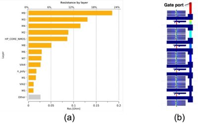
Figure 5 shows the results of gate resistance simulation using ParagonX software. A Pareto chart (Figure 5a) with resistance contributions by layer helps identify the most important layers for gate resistance. The visualization of contributions by layout polygons (Figure 5b) to the gate resistance immediately points to the choke points, or bottlenecks for gate resistance, that are very useful in guiding layout optimization efforts.

Figure 5. Simulation results of gate resistance: (a) gate resistance contribution by layer, and (b) contribution by polygons shown by color over the layout
Gate Resistance in FinFETs
In planar MOSFETs, the gate has a very simple planar structure, and the current flow in the gate is one-dimensional along the direction of the gate width.
In fin field-effect transistor (FinFET) technologies, the gate wraps around very tall silicon fins, leading to a complicated 3D structure. Further, the gate material is selected based on the work function, or the minimum thermodynamic work needed to remove an electron from a solid to a point in the vacuum immediately outside the solid surface, to tune the threshold voltage. The threshold voltage in FinFETs is tuned not by the channel doping, but by gate materials. These materials have very high resistance, much higher than solicited poly (which has typical sheet resistivity of ~10 ohm/sq). Also, the gate may be formed by multiple layers, such as an interface layer with silicon and one or more layers above it.
However, using parasitic extraction software, all these details are hidden from the IC designers and layout engineers. They see the usual polygons for "poly" and for "active,” which makes design work much easier.
Vertical Component of Gate Resistance
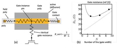
In pre-16-nm technologies, gate resistance was dominated by lateral resistance. However, in advanced technologies, multiple interfaces between gate material layers lead to a large vertical gate resistance. This resistance is inversely proportional to the area of the gate poly. It can be modeled as an additional resistor connecting a gate instance pin to the center point of the gate poly, as shown in Figure 6a. As a result, when the gate gets narrower (e.g., has a smaller number of fins), gate resistance goes down, but gate resistance increases at very small gate widths, as seen in Figure 6b.2 It displays a characteristic nonmonotonic behavior. The old rule of thumb where "the narrower gate has lower gate resistance" does not work anymore. Designers and layout engineers have to select the optimum (nonminimal) gate width (number of fins) to minimize gate resistance.

Figure 6. (a) Gate model accounting for vertical gate resistance, and (b) measured and simulated gate resistance versus number of fins (from [2])
Technology Trends
As we have seen, with technology scaling to ever-smaller nodes (reaching as low as 2 nm at present), both gate resistances and interconnect resistances increase significantly — by up to one or two orders of magnitude. As a result, the details of the layout that were not important for gate resistance in older nodes become very important in advanced nodes. This trend will continue as node dimensions continue to decrease. To understand the equivalent, effective gate resistance values at these levels requires parasitic extraction software such as ParagonX software because SPICE models are no longer effective at these levels.
Learn more about ParagonX software to improve your IC design flow.
References
1. B. Razavi, et al., "Impact of distributed gate resistance on the performance of MOS devices," IEEE Transactions on Circuits and Systems I: Fundamental Theory and Applications, vol. 41, pp. 750-754, 11 1994.
2. A.J.Sholten et al., "FinFET compact modelling for analogue and RF applications," IEDM 2010, p. 190.


