As an experienced semiconductor engineer or designer, imagine producing a symmetrical net layout for a new integrated circuit (IC) but finding a false electrical mismatch in your post-layout SPICE simulations. This nonintuitive result sends you back to the design to check for assymetries, but you find none. What, exactly, is going on here?
It turns out that this false electrical mismatch effect is caused by the difference in distributions of parasitic coupling capacitors over the nodes of parasitic resistor networks. This, in turn, is caused by artifacts of parasitic extraction and parasitic extraction tools.
Here we give you practical recommendations to identify these false mismatch conditions and distinguish them from real mismatches due to layout differences. Ansys ParagonX parasitic extraction software can help you avoid these artifacts and ensure the trustworthiness of post-layout simulations and IC design flow.
Device and Net Matching in IC Design
Many analog and radio frequency (RF) integrated circuits rely on the concept of device and net matching.1,2 Examples of such circuits are StrongARM latches, sense amplifiers, differential pairs, current mirrors, multiphase clocks, and many others. Matched nets and devices give you some wiggle room, ensuring that a circuit will be able to handle unavoidable process variations.
To approach perfect net matching, designers create symmetrical layouts by flipping the design around the X or Y axis, or by shifting or rotating a cell, as shown in Figure 1.
But perfect symmetry and matching are rarely achievable due to constraints of design rules, wire routability, and geometry. That’s why you perform parasitic extraction to verify matching, followed by post-layout circuit simulation, as part of a standard post-layout design flow. If simulations show good, expected results, you have achieved the best symmetry and matching possible. If there are some offsets, mismatches, or differences in measured signals, the matching is not good enough, and the layout needs to be improved.
The Real Problem
Here’s the real conundrum: Even when the nets are perfectly symmetrical and matched, post-layout simulations very often show differences in electrical behavior. A typical scenario is when two nets show a good match for capacitance and resistance but have a large mismatch for RC delay, symbolized by τ (Greek lowercase tau). Common sense and a basic knowledge of physics indicate that the delays should match if capacitances and resistances are matched. The delay mismatch is counterintuitive in this scenario.
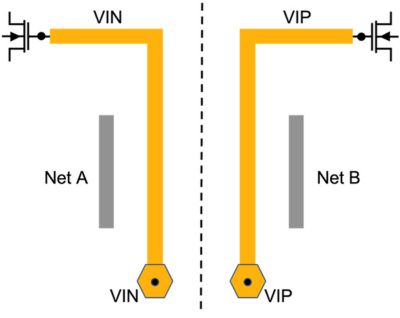
Figure 1. Layout of matched nets VIN and VIP. Input ports are VIN and VIP, and destination points are the gates of the MOSFETs. The nets and their environment are created symmetrically to ensure parasitic resistance, coupling capacitance, and RC delay matching.
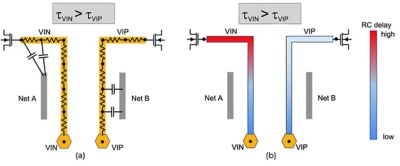
Figure 2. (a) Visualization of parasitic elements (resistances and capacitances). Note the asymmetry, a difference in the distributions of coupling capacitances for nets VIN and VIP. (b) Visualization of RC delay over the net layout. Since coupling capacitances are concentrated at the far end (form the port VIN) of the net VIN and at the near end of net VIP, the delay on VIN is larger than delay on VIP.
The problem, it turns out, is in the parasitic extraction software. Specifically, the root cause of the delay mismatch is related to how parasitic extraction tools distribute coupling capacitances over the nodes of the resistive networks. For some reason, the distribution of coupling capacitances is very asymmetric, as shown in Figure 2.
The most likely reason for such asymmetry is the anisotropy of computational geometry algorithms used by extraction tools. These algorithms — such as sweep (or scan) line or polygon boundary traversing — have a preferred direction, such as left-right, or top-bottom, or clockwise-counterclockwise. So, the algorithms are treating the layout as a flat system instead of a 3D one. This causes the system to lose the natural hierarchy and cell transformation characteristics that, theoretically, can be used to transform the preferred directions.
To investigate this hypothesis, a series of experiments were performed by analyzing post-layout netlists and performing post-layout simulations for several GDS files. The original DSPF file was used as a reference and compared with DSPF files obtained by various transformations — symmetry reflection with respect to the X and Y axes, and by rotations of 90, 180, and 270 degrees. The results for symmetry transformation are illustrated in Figure 3.
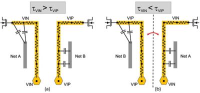
Figure 3. RC parasitic for the (a) original and (b) flipped GDS files. The distributions of coupling capacitances for nets VIN and VIP are reversed for cases (a) and (b). The distributions of coupling capacitances are the same for the left net and the same for the right net for cases (a) and (b).
As expected, the distribution of coupling capacitances is the same for the left net for the original and for the flipped layout. This distribution is also the same for the right net. However, since nets VIN and VIP changed sides in going from the original to the flipped layout, the distributions of coupling capacitance on net VIN for case (a) now becomes the distribution of coupling capacitances for net VIP for case (b), and vice versa.
This change in capacitance distributions correlated very well with the simulated RC delays on VIN and on VIP. RC delay, τ, is larger for net VIN than for VIP in case (a), but smaller than the RC delay on VIP in case (b). Similarly, we observed a difference in post-layout circuit simulations, showing a significantly larger transition time for nets VIN in case (a) and smaller for case (b) than the transition time on net VIP. This shows that the electrical mismatch between symmetric nets VIN and VIP is an artifact of parasitic extraction tools, as explained above.
Of course, if the difference in couplings and in RC delays for nets VIN and VIP does not change its sign after performing a transformation of the layout, such a difference is caused by real layout mismatch that needs to be fixed on the layout.
Coupling Capacitors Distribution Over Parasitic Resistor Network
This experiment may be the first time any group has investigated the artifacts of parasitic extraction related to anisotropic, asymmetric distribution of coupling capacitances for symmetric layout.
False mismatch effects were observed for different designs, technologies, foundries, and three major parasitic extraction tools. The severity of false anisotropy is different for different extraction tools. This may be explained by a difference in the quality of coupling capacitors distributions for the three parasitic extraction tools, ranging from accurate to crude to very crude, as shown in Figure 4.
Every parasitic extraction tool tries to minimize the size of the parasitic RC network to enable fast post-layout simulation times (for SPICE, EMIR, timing, and other tools). There is always a trade-off between the netlist size (simulation time) and accuracy. Different parasitic extraction tools do this with a different level of physics awareness, and with a different level of accuracy.
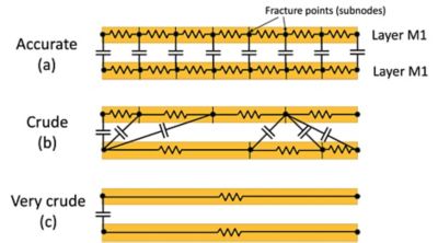
Figure 4. Distribution of coupling capacitances over the nodes of parasitic resistor networks. Case (a) is the most accurate, case (b) is less accurate, and case (c) is very crude.
Simulation and Analysis Results
Post-layout SPICE simulation of a StrongARM latch3 (see Figure 5) implemented in 5-nm FinFET technology revealed a mismatch of transition times for devices M1 and M2 of ~500 fs, which was much higher than the upper limit spec for this mismatch (~30 fs). The layout was relatively small, and its visual inspection did not reveal any asymmetries. Designers and layout engineers did several iterations of the layout, trying to get rid of the mismatch in simulations. This took them more than two weeks, without success.
Flipping the layout around the Y axes resulted in a post-layout netlist that showed a mismatch with an opposite sign: –370 fs. This result is a clear, convincing argument that this mismatch of +500/-370 fs is caused by an artifact of the parasitic extraction tool.
Analysis of net mismatch using the ParagonX electronic design automation (EDA) tool confirmed a large RC delay difference of over 15% between nets in1 and in2. This difference changes its sign for the original and flipped layouts. Subsequent visualization of coupling capacitances using ParagonX software further confirmed a strong asymmetry of their distributions. (These plots cannot be shown in this blog for third-party confidentiality reasons.)
Interestingly, both resistances and net-to-net coupling capacitances for nets in1 and in2 were matched to a very high accuracy. Resistances were matched better than 0.05%, and coupling capacitances were matched better than 0.2%. This is a common effect we observed in many post-layout netlists — while capacitances and resistances on matched nets are very close, RC delays may be quite different because of the effect discussed in this blog.
It is believed that the 0.2% of capacitance difference is caused by the inaccuracy of rule-based (pattern-matching based) capacitance extraction. A much higher accuracy in capacitance extraction can be obtained using random-walk based field solvers (FS) with user-controlled accuracy goal settings. It is always recommended to use selected net FS extraction mode for nets whose capacitive matching (or binary or nonbinary weighting for capacitor arrays in SAR ADC) is critical for the circuit operation.
Discussing the Results
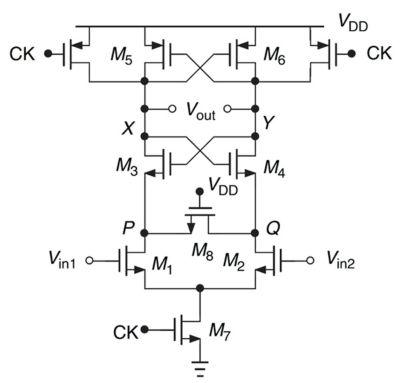
Figure 5. Schematic of StrongARM latch. Nets in1 and in2 should be matched for RC delay.
Post-layout circuit simulation is considered a gold standard for analyzing and simulating custom transistor-level IC designs. The observed false mismatch effect leads to an interesting question: How accurate is post-layout simulation? Obviously, post-layout simulation accuracy cannot be higher than the parasitic extraction tool’s accuracy. And while capacitance and resistance extraction are, in general, quite accurate, a crude distribution of coupling capacitances over the nodes of parasitic resistors network may lead to errors of ~500 fs (or more) in transient and AC simulations. This finding may have important implications for the trustworthiness and accuracy of SPICE simulations for precision and high-speed analog designs, timing analysis, and other applications. At a minimum, the industry needs to establish a methodology for detecting, debugging, resolving, or getting around this problem.
Just as importantly, false mismatches induced by extraction artifacts may mask a real layout and electrical mismatch, caused by the differences in layouts and contexts of matched nets. Detecting a real mismatch becomes difficult or even impossible in the presence of false mismatches. Also, a real mismatch may look like zero or small mismatch if false and real mismatches coincidentally cancel each other, which is also a high-risk factor.
Practical Recommendations
Consider the following recommendations:
- For circuit designers and layout engineers:
a. Pay more attention to mismatches in general and false mismatches caused by incorrect parasitic extraction in particular.
b. Increase the awareness of these effects. Request that EDA tool vendors improve the accuracy and get rid of such artifacts in parasitic extraction related to coupling capacitors distribution.
c. Use a field solver for accurate, controlled capacitance extraction of matched nets (if capacitance matching is critical).
d. Use ParagonX software or other EDA tools to proactively check and verify net and device matching in post-layout netlists, debug such problems, and improve the layout matching.
- For EDA tool vendors: Improve the accuracy of parasitic extraction tools and, in particular, improve the quality of coupling capacitors distribution.
- For foundries: Perform more thorough verification and qualification of parasitic extraction tools related to net matching and to the quality of coupling capacitors distributions.
- For EDA researchers: Come up with better algorithms and methodologies to improve the accuracy of post-layout netlists without exploding their size.
- For all: Check for false mismatches in your design flow that could be introduced by parasitic extraction:
a. Create layouts by applying symmetry transformation to the original layout (see Figure 6), such as:
i. Flip around the X axis.
ii. Flip around the Y axis.
iii. Rotate by 180 degrees, and by 90 or 270 degrees (if DRC allows that).
b. Perform parasitic extraction.
c. Use ParagonX software to compare post-layout netlists for the original and transformed layout.
i. ParagonX software detects and debugs mismatches much faster and easier than SPICE.
d. If ParagonX software is not available, use post-layout SPICE simulation or another analysis tools (STA, etc.) to compare the two post-layout netlists.
e. In the case of significant differences that are indicative of false mismatches:
i. Perform visual inspection of the layouts (if possible).
ii. Report findings to parasitic extraction tool vendors and to foundries.

Figure 6. Layout transformations that can help identify a false net mismatch. Electrical characteristics are invariant with respect to these transformations, so parasitic capacitances, resistances, delays, devices, and SPICE simulations should be invariant as well.
Learn more about how Ansys ParagonX IC layout parasitics analysis and debugging software can help you solve the problem of false electrical mismatches in your IC designs.
References
[1] “The art of analog layout,” 2nd ed., A. Hastings, Prentice Hall, 2005.
[2] “CMOS IC Layout: Concepts, Methodologies, and Tools,” D.Clein, Newnes, 1999.
[3] “The StrongARM Latch” (A Circuit for all seasons), B.Razavi, IEEE Solid-State Circuits Magazine, v. 7, no.2, p. 12-17, 2015.
Just for you. We have some additional resources you may enjoy.
Learn More
See how Ansys ParagonX IC layout parasitics analysis and debugging software can help you solve the problem of false electrical mismatches in your IC designs.


