


Topic Details
- What Is Advanced Semiconductor Packaging?
- Advantages of Advanced Semiconductor Packaging
- Applications for Devices Using Modules Made With Advanced SemiconductorPackaging
- Advanced Packaging Components and Technologies
- Challenges in Advanced Semiconductor Packaging
- The Future of Advanced Semiconductor Packaging
What Is Advanced Semiconductor Packaging?
Advanced semiconductor packaging is a collection of manufacturing processes combining multiple semiconductor chips into a single electronics package. This approach increases capability and reduces power consumption and cost.
Traditional packaging is like building a single one-story building on a plot of land. Advanced packaging allows you to place several buildings on a smaller piece of land and connect them with bridges, shafts, and tunnels. Companies that effectively leverage these techniques will gain a competitive advantage in the rapidly growing semiconductor market.
The most common techniques used in advanced packaging are 2.5D, 3D-IC, heterogeneous integration, fan-out wafer-level packaging, and system-in-package. Each is a different way to take a single chip from a wafer and place it with others in a single, electrically connected assembly surrounded by plastic, metal, or glass — a package. Once created, a package is connected to a printed circuit board (PCB) or flexible tape and placed into an electronic device.
Advantages of Advanced Semiconductor Packaging
The ability to pack more transistors into less space is slowing as semiconductor technology starts to run up against the laws of physics. For decades, the microelectronics industry has used Intel co-founder Gordon Moore’s prediction that the density of transistors in chips will double every two years, referred to as Moore’s Law, to guide its investments and planning to keep up with this pace. This drives each generation of chips to smaller feature sizes and greater densities, making electrical connections in devices a performance bottleneck. .
Advanced packaging is a powerful way for designers to overcome this limitation. They can remove bottlenecks and decrease costs by arranging multiple chips in three dimensions and building connections directly between chips and in transitional integrated circuits. An added benefit is placing chips with different functions nearby, thus decreasing power consumption, increasing speed, and simplifying multi-function devices into a single package.
This form factor of a single package also reduces manufacturing, shipping, and inventory costs by moving the integration from a post-processing step involving multiple components to a front-end step at the semiconductor manufacturing site, also referred to as the fab. This approach also significantly reduces packaging labor costs, removing the need for separate packaging facilities in locations with low labor costs.
Applications for Devices Using Modules Made With Advanced SemiconductorPackaging
With the growing demand for computing power and memory to store all the data people create there is a need for more efficient and inexpensive microelectronic devices. More sophisticated and capable consumer electronics also create a market for greater functionality in smaller packages with less power consumption. More and more devices are becoming smarter, adding components that measure (sensors), import data, calculate (processor), store data (memory), or export data. Advanced packaging can help a product combine multiple instances of each function into a single module.
One of the fastest-growing areas for this is the automotive industry. Advanced systems for performance, efficiency, and safety — combined with an ever-increasing number of sensors — are pressuring the demand for more robust, efficient, and inexpensive electronic modules made with advanced packaging.
Internet-of-Things (IoT) devices are another example of a product designer’s desire to combine multiple electronic functions in a single part to add to their electronic design. A solution created with advanced packaging simplifies the automation of assembly and the complexity of the PCB while increasing performance and decreasing cost and power needs.
Advanced packaging is helping to realize the intense computing demands of artificial intelligence (AI) and high-performance computing (HPC). This approach delivers more capability in a smaller, less power-hungry configuration. Providers of the hardware for AI and HPC, like NVIDIA, have established advanced packaging supply chains. They have turned to Intel and TSMC’s advanced packaging capabilities to produce the multi-function modules they need to increase performance while keeping power needs and costs under control.
Advanced Packaging Components and Technologies
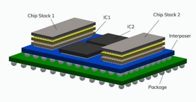
Advanced semiconductor packaging uses multiple technologies to more efficiently combine IC chips in a package.
A good place to start understanding advanced packaging is to look at its components and the various advanced packaging technologies that semiconductor foundries use.
Components
- Chiplet: An unpackaged discrete die optimized for a given function combined with other chiplets and multi-function IC chips at the package level.
- Die:. A block of semiconductor material cut from a larger wafer that contains circuits designed to perform one or more functions. When dies are connected to a substrate or other dies, they become a chip.
- I/O Pads or Bumps: Conducting areas on the surface of a chip used to send signals in or out of the chip.
- Interconnect: A structure that connects two or more circuit elements to transfer an electrical current between them. It’s usually a thin structure connecting one or more dies.
- Interposer: A layer of material between one or more chips and a substrate. In advanced packaging, the material can be silicon or glass-based.
- Printed Circuit Board (PCB): A flat structure that can be rigid or flexible with multilayer circuits that electrically connect the components in an electronic system. They are usually made from FR4 when rigid or polyamide when flexible.
- Redistribution Layer (RDL): An extra metalized layer under a die or dies that contains internal conducting paths that create more advantageous I/O pads.
- Solder Ball: A small ball of solder used to connect components in a semiconductor package. Its size varies depending on what it connects.
- Substrate: A flat component containing circuits that physically and electrically connect other components in a package. An IC substrate is a layer of semiconductor material and a laminate substrate made out of FR4 or polyamide.
- System-on-Chip (SoC): An IC chip that integrates all computer or electronic system functions on a single chip.
- Through Silicon Via (TSV): An electric connection between the top and bottom of a silicon wafer or die. This turns a thin semiconductor material into an interconnect between components.
- Wire Bond: A wire between a die and a substrate or between multiple dies. This relatively inexpensive method of connecting components in a package dominates traditional packaging.
Technologies
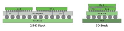
2.5-D Stacks use an interposer with TSVs to attach multiple chips to the package, and a 3D stack uses TSVs designed into the dies to stack dies vertically.
- 2.5-D: Instead of attaching multiple dies to an IC substrate, 2.5-D technology uses an interposer between the dies and the substrate. The interposer uses TSVs to pass signals through the interposer.
- 3D-IC: A method in which multiple dies are stacked on top of each other. TSVs connect the dies.
- Fan-Out Wafer-Level Packaging: An RDL transitions from dense I/O pads on the chip to a larger ball grid array on the substrate.
- System-in-Package (SiP): 2.5D or 3D-IC technologies are used to produce a complete computer or electronic device package. Instead of placing all the ICs needed for a SoC solution, SiP combines multiple dies to achieve the same behavior in a single package.
Challenges in Advanced Semiconductor Packaging
From packing a suitcase to creating the latest GPU modules, packaging is about fitting everything you need in your space as efficiently as possible. For advanced semiconductor applications, you must also deal with power integrity, signal integrity, thermal integrity, and mechanical stress issues while maintaining cost goals.
Interconnects
Each chip in a package needs to be connected and to the I/O pads that connect the module to the rest of the electronic device. Conductive pathways, such as interconnects, TSV, or wires, must be designed into the package. Because they carry a signal, each pathway must be checked to ensure its signal does not interfere with its neighbors and doesn’t heat up too much.
Power
Power efficiency is a driving differentiator in the market. Customers want to do more with less power, so package designers must develop configurations and leverage technologies that minimize power consumption and loss.
Heat
Every component in the package can generate heat when current is applied. The package needs thermal management solutions that leverage configuration and materials that minimize heat buildup, transfer the heat away from components, and how it impacts the devices used.
Robustness
The materials expand and contract when a package heats up and cools down. Designers must use various materials and interconnect technologies to ensure the difference in expansion for each material and the repeated growing and contracting do not cause failure in any of the interconnects or chips. Understanding solder ball fatigue and the package design must also survive the wear and tear of harsh environments in applications such as automotive, IoT, and aerospace.
Cost
In the competitive semiconductor industry, cost is a major driver. As backend process packaging, traditional chip packaging can be labor-intensive and include transportation costs. Advanced packaging processes must leverage automation and move packaging to be part of the upfront processes, including integrated testing. Designers often leverage optimization tools to choose their options intelligently with cost in mind.
The Future of Advanced Semiconductor Packaging
Up and down the semiconductor supply chain, companies are developing roadmaps that include more advanced packaging, increased performance, and lower costs. A recent study by Yole Intelligence found that in 2022, advanced packaging was 48% of the $92 billion industry. The report predicts the share will grow to 58% of a $136 billion industry by 2028.
Next-generation packaging manufacturing must leverage new materials, greater automation, and innovative technologies to meet the increased demand for power-efficient and affordable packages, more compact chip designs, and system-in-chip applications.
Competition in the packaging ecosystem between countries and companies will be intense. The 2023 CHIPS Act includes $3 billion in funding for the National Advanced Packaging Manufacturing Program. Industry leaders Intel, TSMC, and Amkor announced $3.5, $2.9, and $2 billion investments in 2023, respectively, to develop new advanced packaging facilities.
Beyond the technologies in the manufacturing plant, engineers will be looking for better software tools that support specific packaging technologies that can be integrated into the design workflow. For example, Ansys, Microsoft, and TSMC recently collaborated on a cloud-based stress simulation toolset for 2.5D/3D-IC packaging.