


Webinar
Ansys-Synopsys Technology Update: The Latest Advances in Multi-Die Design
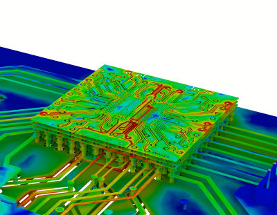
The semiconductor industry is rapidly adopting 2.5D and 3D multi-die designs as the significant benefits have become clear for applications like HPC, GPU, mobile, and AI/ML. Multi-die design technology has been quickly evolving and early experiences have led to the development of more advanced implementation and analysis techniques.
Synopsys and Ansys have created a unified design flow that carries designers from early exploration to implementation, to final signoff. They are deeply engaged with semiconductor designers on advanced multi-die projects and have helped customers bring successful designs to market.
What You will Learn:
- Multi-die design best practices for thermal, signal, and power integrity
- Insights from practical multi-die design case studies
- More advanced packaging technologies for thermal management, backside power, and co-packaged optics