


Case Study
“Ansys Lumerical simulation software met our criteria for accuracy, compatibility, user-friendliness, and support, and enabled us to design and optimize our photonic devices with confidence. The software made it easy to integrate fabrication process data for practical and realistic simulation results. Additionally, the software's customizability allowed us to tailor complex designs to our specific needs while leveraging advanced optimization methods. The quality technical support and resources ensured we got the most out of the software.”
— Mariam Aamer Benelfaquih, Senior R&D Photonics Design Engineer, LIGENTEC
The advancement in photonic integrated circuit (PIC) technology and applications is ushering in each new generation of photonics products with increasing performance criteria and complexity. Meeting demanding performance and complexity requirements while ensuring manufacturability and yield is a critical challenge faced in the PIC industry.
Challenges
The design process can be challenging, time-consuming, and expensive, as it involves multiple iterations, fabrication, and testing. LIGENTEC is interested in optimizing complex PICs and photonic devices to meet specific performance criteria, including an optimized waveguide crossing with multiple figures of merit such as low insertion loss, minimum back-reflection, compact footprint, and low crosstalk.

Engineering Solution
LIGENTEC used Photonic Inverse Design (PID) capabilities in Ansys Lumerical FDTD for the design and optimization of its waveguide crossing. The company’s engineering solution involved specifying the initial geometry of the structure, defining the simulation parameters and material properties, setting the design objectives and constraints, and running the optimization algorithm to generate an optimized design.

Benefits
- Customization of design optimization goals and constraints.
- Co-optimization of multiple figures of merit, including insertion loss, footprint, and crosstalk.
- Increased design cycle efficiency by combining an efficient and fast varFDTD method together with a powerful 3D FDTD method from Lumerical and its seamless integration with PID optimization.
- Explored a very large design space and identify optimal designs that would be extremely difficult and time-consuming to find using traditional optimization methods. Lumerical varFDTD allowed for fast exploration of the design space and high-accuracy results were then extracted from full 3D FDTD simulations.
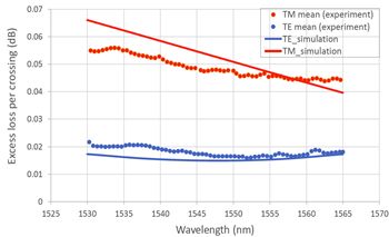
- Designed a new waveguide crossing was with a 4X reduction in footprint while maintaining a low loss performance of ~0.02dB/crossing and crosstalk <-60dB.
- Process variation analysis achieved manufacturable designs with robustness to 3σ process variation.
- Allowed for a script-based conversion of the optimized design in a computer-aided design (CAD) environment to a physical mask layout (.gds file) that can be manufactured by a foundry as per their process.
- This workflow streamlined the company’s gds layout generation and eliminated any sources of errors.
- Accurately optimized and predicted the performance of the design, as shown in the measurement plot.
- Ability to consider the impact of process variation and its limitations to identify potential issues early in the design process, resulting in first time-right designs and thereby eliminating the need for design iterations and minimizing the risk of expensive fabrication failures.
Let’s Get Started
If you're facing engineering challenges, our team is here to assist. With a wealth of experience and a commitment to innovation, we invite you to reach out to us. Let's collaborate to turn your engineering obstacles into opportunities for growth and success. Contact us today to start the conversation.