-
United States -
United Kingdom -
India -
France -
Deutschland -
Italia -
日本 -
대한민국 -
中国 -
台灣
-
Ansys is committed to setting today's students up for success, by providing free simulation engineering software to students.
-
Ansys is committed to setting today's students up for success, by providing free simulation engineering software to students.
-
Ansys is committed to setting today's students up for success, by providing free simulation engineering software to students.
-
Contact Us -
Careers -
Students and Academic -
For United States and Canada
+1 844.462.6797
DATE: 6/8/2022
PRESS RELEASE
Ansys Significantly Increases Speed and Capacity of Semiconductor Signoff with Massively Scalable SeaScape Platform
New products Ansys® Totem-SC™ and Ansys® PathFinder-SC™ optimize power and reliability for automotive, 5G, and high-performance compute semiconductors
Key Highlights
- Totem-SC delivers next-generation power integrity analysis for analog, mixed-signal, memory, and image sensor designs.
- PathFinder-SC delivers advanced semiconductor reliability analysis for all semiconductor design types, including AI/ML, mobile and high-performance compute
- SeaScape is an open and extensible platform for semiconductor multiphysics, and massively scalable for elastic compute, big data analytics and AI/ML
PITTSBURGH, PA, June 8, 2022 – Ansys (NASDAQ: ANSS) announced the release of two new semiconductor products – Ansys® Totem-SC™ and Ansys® PathFinder-SC™ – for power integrity and electrostatic discharge (ESD) reliability signoff, respectively. The new products significantly increase the speed and capacity of existing Totem™ and PathFinder™ products by integrating them into the Ansys SeaScape™ big-data platform for distributed processing. This deepens Ansys’ strategic commitment to adopting open and customizable design platforms to enable multiphysics engineering simulations.
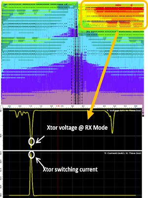
Totem-SC is built on the SeaScape platform to address the growing challenge of power integrity analysis in today’s extremely large memory and analog mixed signal designs. SeaScape is a massively scalable data platform that used big-data techniques to enable highly scalable elastic compute and facilitate multiphysics analyses. Totem-SC delivers 10x faster performance on average for dynamic voltage drop signoff of next generation designs like complementary metal oxide semiconductor (CMOS) image sensors, dynamic random-access memories (DRAM), flash memories, field programmable gate arrays (FPGAs), and high-speed transceivers.
“Power supply noise is a critical metric for our CMOS image sensors as it directly impacts pixel performance,” said Seonil Brian Choi, Corporate VP Samsung Electronics. “Totem-SC offers us a high-capacity IR signoff solution for Samsung’s high-resolution sensor designs using standard low-memory machines. The high-fidelity results give our team the confidence to maximize design optimization for a better final product.”

Ansys Totem-SC showing region of voltage drop in the power grid
PathFinder-SC provides a high-capacity solution for verifying the protective circuitry found on all chips that protect them from electrostatic discharge (ESD) and damage from voltage spikes. This technology has become increasingly pivotal as silicon technology continues to shrink to 7nm and below where these tiny transistors need to be protected by critical ESD circuitry that is checked, verified, and signed off with PathFinder-SC. SeaScape technology allows PathFinder-SC to deliver 10x faster turnaround for ultra-large SoCs, which makes it ideal for today’s large, high-speed semiconductor designs in artificial intelligence, imaging, networking, and 5G and 6G telecommunications.
“ESD signoff has become increasingly challenging as our design has grown larger and the predictive accuracy requirements have tightened,” said Chanhee Jeon, Master (VP of Technology) at Samsung Electronics. “We have found that PathFinder-SC gives us a high-capacity ESD signoff solution with superior root-cause analysis and multiphysics analysis capabilities, which helps us meet our delivery schedules.”
SeaScape’s big-data elastic compute algorithms are ideal for scalable, distributed deployment as it uses regular sized machines and does not require a large master node with huge memory. The SeaScape platform is an open platform architecture that allows customers to integrate other tools and their own algorithms by means of a Python-based customizable user interface (UI)
“Designing today’s chips and electronic systems is an increasingly complex multiphysics analysis and simulation problem that requires a broad array of tools to solve,” said John Lee, vice president and general manager of the electronics, semiconductor, and optics business unit at Ansys. “Ansys strongly believes in providing open and extensible platforms like SeaScape so our users can use the best tools to simulate, analyze, and optimize their product designs – all the way from early prototyping to manufacturing signoff.”
About Ansys
If you've ever seen a rocket launch, flown on an airplane, driven a car, used a computer, touched a mobile device, crossed a bridge or put on wearable technology, chances are you've used a product where Ansys software played a critical role in its creation. Ansys is the global leader in engineering simulation. Through our strategy of Pervasive Engineering Simulation, we help the world's most innovative companies deliver radically better products to their customers. By offering the best and broadest portfolio of engineering simulation software, we help them solve the most complex design challenges and create products limited only by imagination. Founded in 1970, Ansys is headquartered south of Pittsburgh, Pennsylvania, U.S.A. Visit www.ansys.com for more information.
Ansys and any and all ANSYS, Inc. brand, product, service and feature names, logos and slogans are registered trademarks or trademarks of ANSYS, Inc. or its subsidiaries in the United States or other countries. All other brand, product, service and feature names or trademarks are the property of their respective owners.
ANSS-T
Let’s Get Started
If you're facing engineering challenges, our team is here to assist. With a wealth of experience and a commitment to innovation, we invite you to reach out to us. Let's collaborate to turn your engineering obstacles into opportunities for growth and success. Contact us today to start the conversation.


