


WHITE PAPER
3D Heterogenous Integration: Design and Verification Challenges
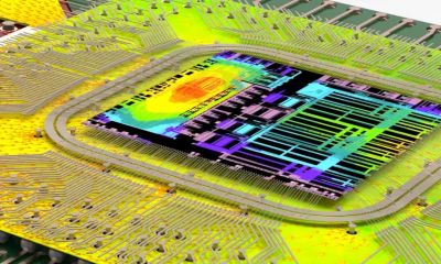
Next-generation semiconductor products increasingly rely on vertical integration technologies to drive system density, speed, and yield improvement. Due to the increased coupling effects across multiple physics, co-simulation and co-analysis of these phenomena are critical for a robust chip-package-system design. Advanced 2.5D/3D-IC systems are constructed with multiple dice, interposers, packaging layers, and connection substrates, which make the coupling effects even more of a challenge. The advent of multi-die heterogeneous integration (HI), integrating chiplets with different process technologies and electrical characteristics, requires additional design and verification capabilities going beyond any existing design tools and flows. From system-in-package (SiP) to 2.5D-IC with interposer-enabled advanced packaging and true 3D-IC with stacked dies/chiplets, the emerging interconnect architecture of both signal nets and power delivery network call for an innovative electronic design automation (EDA) solution with ultra-large data capacity and highly scalable compute technology.