


Resistance and current density checks are useful and necessary steps for electrostatic discharge (ESD) verification, but proper care must be taken when setting up the simulations. Parasitic extraction tools on standard post-layout netlists sometimes yield calculated resistances that are higher or lower than actual values by a factor of up to 100 times, which is a huge discrepancy. Current densities can also be significantly off. These problems are especially severe in the latest sub-10-nm technology — nodes with high interconnect resistances. Relying on such simulations leads to either missed ESD problems or to wasted time trying to fix artificial errors on a good layout.
Fortunately, the causes of these discrepancies are understood and can be easily corrected using proper simulation procedures. While it seems obvious that simulation conditions should mimic and reproduce the realistic current flow over and near the devices to avoid parasitic extraction and simulation artifacts, these conditions are sometimes not met, leading to the errors discussed above.
The two most common root causes of such errors are:
- Artificially high resistance values caused by the incorrect treatment of a distributed ESD diode as a cell with a single instance pin
- Artificially low resistance values caused by connecting an ESD diode with a port by a small (1-milliohm, or mΩ) resistor
ESD Workflow Overview
Resistance checks and current density checks are often performed on post-layout netlists to verify ESD protection networks (see Figure 1).1 Point-to-point (P2P) resistance is used as a proxy, or a figure of merit, for the quality of metallization, and as a proxy for ESD stress voltage. High P2P resistance values (e.g., higher than 1 Ω) indicate problems with the metallization and should be debugged and improved.
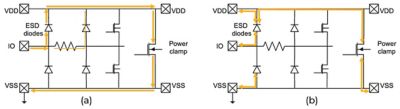
Figure 1. (a) ESD current paths, and (b) P2P resistances (red arrows) in ESD protection network. Resistances between pads and ESD diodes, diodes to power clamps, and other resistances are calculated to verify robustness and quality of ESD protection.
In recent years, many fabless semiconductor design companies have reported puzzling problems with ESD resistance and current density simulations when post-layout netlists generated by standard parasitic extraction tools are used. These problems became especially severe in the latest sub-10-nm nodes with high interconnect resistances.
The problems of unreasonably large or low (by ~100 times) resistances between ESD diodes and pads or power clamps, and unphysical current densities in the interconnects, usually happen when fabless semiconductor design companies use ESD diode parametrized cells (p-cells) provided by the foundries. The cells are designed, verified, and qualified by the foundries and should be good. However, the quality of the connections of these ESD cells to the power nets and to IO nets can be poor. Such poor connections can lead to high resistances and current densities, which lead to big ESD problems. That’s why, even when ESD cells themselves are high quality, the resistance and current density checks on the complete ESD network are required.
Artificially High Resistance Case Caused by a Single Instance Pin
In foundry-provided process design kits (PDKs), ESD diodes are often represented as p-cells with a single instance pin for each of the terminals: anode and cathode. This differs from how power clamp metal–oxide–semiconductor field-effect transistors (MOSFETs) are usually treated in the PDK, in which each individual finger of a multifinger device is represented as a separate device instance, with its own instance pins for terminals.
These instance pins are usually used as the origin or the destination for point-to-point (P2P) resistance simulations. As a result, in the case of ESD diode p-cell simulations, current flows into a single discrete point, creating artificial current crowding, high-current density values, and a high spreading resistance, as shown in Figure 2a.
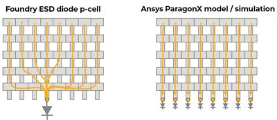
Figure 2. Vertical cross-section of ESD diode showing current flow pattern for simulation using (a) single instance pin and (b) distributing current in a realistic manner over the diode area
These high values are artifacts of simulation, induced by the erroneous representation of a large distributed device by a single discrete instance pin. In real operation, ESD diodes conduct current through all fingers, and the total ESD current is distributed over a large area, more or less uniformly.
Furthermore, in advanced technology nodes with many layers, the lower metal layers have high sheet resistivity. They are used for vertical current routing and contribute little to the total resistance. Contacts and vias above the active device conduct vertical current in parallel and, ideally, in a uniform manner. The current is shared by many contacts and vias, resulting in a low total resistance.
On the contrary, in simulations using a single instance pin as a start point or destination point, the current concentrates and crowds near that instance pin. This creates artificial, unrealistic current flow patterns, such as lateral (instead of vertical) current in lower metal layers (M0, M1, M2, and so on), along with highly nonuniform current in vias and high current density in vias close to the instance pin.
Such behavior leads to an artificially high spreading resistance. Figure 3 compares the results of simulation for a standard ESD diode for 5-nm technology. The resistance calculated using a single instance pin is ~7.65 Ω. The resistance simulated using conditions providing the realistic (distributed) current distribution over the device area is 0.069 Ω — more than 100 times lower.
Furthermore, when trying to determine which layers are causing problems, these two simulation conditions report different rankings of layer contributions to the total P2P resistance. Simulations with single discrete instance pins may lead to a completely wrong layer optimization strategy by focusing on the wrong layers.
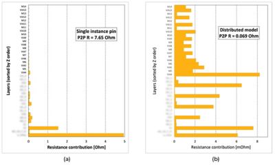
Figure 3. P2P resistance from ESD diode to ground net port and resistance contribution by layer for (a) single instance pin case and (b) distributed simulation conditions
The current density distribution in lower layers also shows a strong current crowding near a single instance pin, as shown in Figure 4. In the case of distributed current flow (Figure 4b), current density is more or less uniform, and its peak value is ~63 times lower than in the single instance pin case.
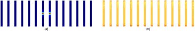
Figure 4. Current density distributions in (a) single instance pin and (b) distributed simulation conditions. Peak current density for the left case (a) is 63 times higher than for the right case (b).
Artificially Low Resistance Case
In some situations, the ESD diode instance pin is connected not to the low-level layers (such as diffusion or contacts), but directly to a port (pin) of a power net, located at the top metal layer. The resistance of this connector resistor is very low, such as 1 mΩ. Why does this misplaced connection happen? One possibility is that the terminal of the ESD diode is mapped to a well or substrate layer that is not extracted for resistance by the parasitic extraction software. As a result, the parasitic extraction tool connects it to a net’s R network at a rather arbitrary point, which turns out to be a port, by a connector resistor. This is similar to how MOSFETs’ bulk terminals are typically connected to the port (because wells and substrates are not extracted for resistance).
Visualization of parasitics and their probing enable engineers to identify such extraction details and understand what’s going on in parasitic extraction and electrical analysis, as illustrated in Figure 5. Such analysis can help them avoid misplaced connections.
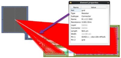
Figure 5. Visualization of parasitics over layout, helping identify connectivity, nonphysical connector resistors, and probe parasitics
Thus, the connectivity of ESD diode to the power net is an error in design. The resistance from the ESD diode to the port of the power net is very low (1 mΩ) due to this connector resistor bypassing the real current path through the interconnects.
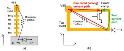
Figure 6. (a) Schematic illustration of a connector resistor connecting ESD diode instance pin with power net port and (b) top-view illustration of real ESD current path from ESD diode to power clamp (shown in green) versus artificial simulated current path
Similarly, the simulated current path from the ESD diode to power clamp differs from the real current path, as shown in Figure 6. The current follows the path of minimum resistance (minimum dissipated power) from the ESD diode to the power net port, then flows along the (low-resistive) top metal and down to the power clamp. Because of this, simulated resistance and current densities are incorrect and do not represent the real resistance and current density.
To properly simulate the resistance and current for this case, the connector resistance has to be removed, and the diode’s instance pin should be connected to the lowest layer in a distributed manner. This is best done by a parasitic extraction tool.
Connector Resistors
Connector resistors are semi-hidden features in parasitic extraction tools. These are nonphysical resistors, i.e., they are not generated by layout shapes and their resistivity. These resistors are not controllable by users. Extraction tool vendors do not educate semiconductor companies about this feature, probably because it’s considered an internal detail of implementation.
Connector resistors are used for various connectivity purposes — for example, to connect instance pins of devices to a resistive network or to other instance pins; to connect disconnected (“opens”) parts of a net; to “short” ports; and for many other purposes. Their value is usually very low, such as 0.1, 1, 10, or 100 mΩ. Most of the time, they do not have a harmful effect on electrical simulation results. However, as discussed above, they can sometimes have a strange or deleterious effect, such as shorting a finite resistance of interconnects or adding 0.1 Ω resistance to a system that has much lower resistance (e.g., power FETs have interconnect resistance values in the range of mΩ).
Being able to understand, identify, and visualize connector resistors on the layout (as shown in Figure 5) and be aware of their presence and potential impact is important to a good understanding of the structure, connectivity, and potential pitfalls in a post-layout netlist. Parasitic extraction simulation can give you this level of understanding.
Learn More About P2P Resistance and Current Density
Clearly, there are simple solutions to correct the bizarre P2P resistance and current density anomalies in ESD network simulations using a proper parasitic extraction simulation tool. One such tool, Ansys ParagonX integrated circuit layout parasitics analysis and debugging software, was used for all simulations and visualizations presented here. Visit that webpage to learn more about how ParagonX software can help you obtain correct resistance and current density values in your ESD circuit designs and avoid the large errors that some semiconductor designers are experiencing.
Reference
“ESD Electronic Design Automation Checks,” Technical report, ESD Association, 2014. Free download: https://www.esda.org/zh_CN/store/standards/product/4/esd-tr18-0-01-14