
WHITE PAPER
Designing for Success: A Solver Combination Strategy for Photonic Integrated Components
With the increasing demand for optical bandwidth, photonic integrated circuit (PIC) technology is undergoing a growth rate very similar to the one seen by electronic integrated circuits over the last half-century. To keep up with the increasing number of components and circuit complexity, efficient and reliable automated design tools are necessary to carry out virtual prototyping, improve yields, lower development costs, and shorten design cycles.
The combination of sub-wavelength features and large device geometries characteristic of integrated optical components can present serious challenges for simulation tools and often force designers into undesirable trade-offs between accuracy and computational time. The need for broadband, bi-directional, or omni-directional propagation can also present additional challenges. In this white paper, we will discuss some approaches for addressing these challenges with a combination of optical solvers.
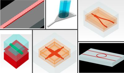
Several application examples including Y-Branch Splitter, Grating Coupler, Bragg Waveguide Grating, and Spot Size Converter are used to demonstrate how and when the following optical mode and propagation methods can be leveraged:
- Finite Difference Time Domain (FDTD)
- 2.5D Variational FDTD (varFDTD)
- Finite Difference Eigenmode (FDE)
- Eigenmode Expansion (EME)